

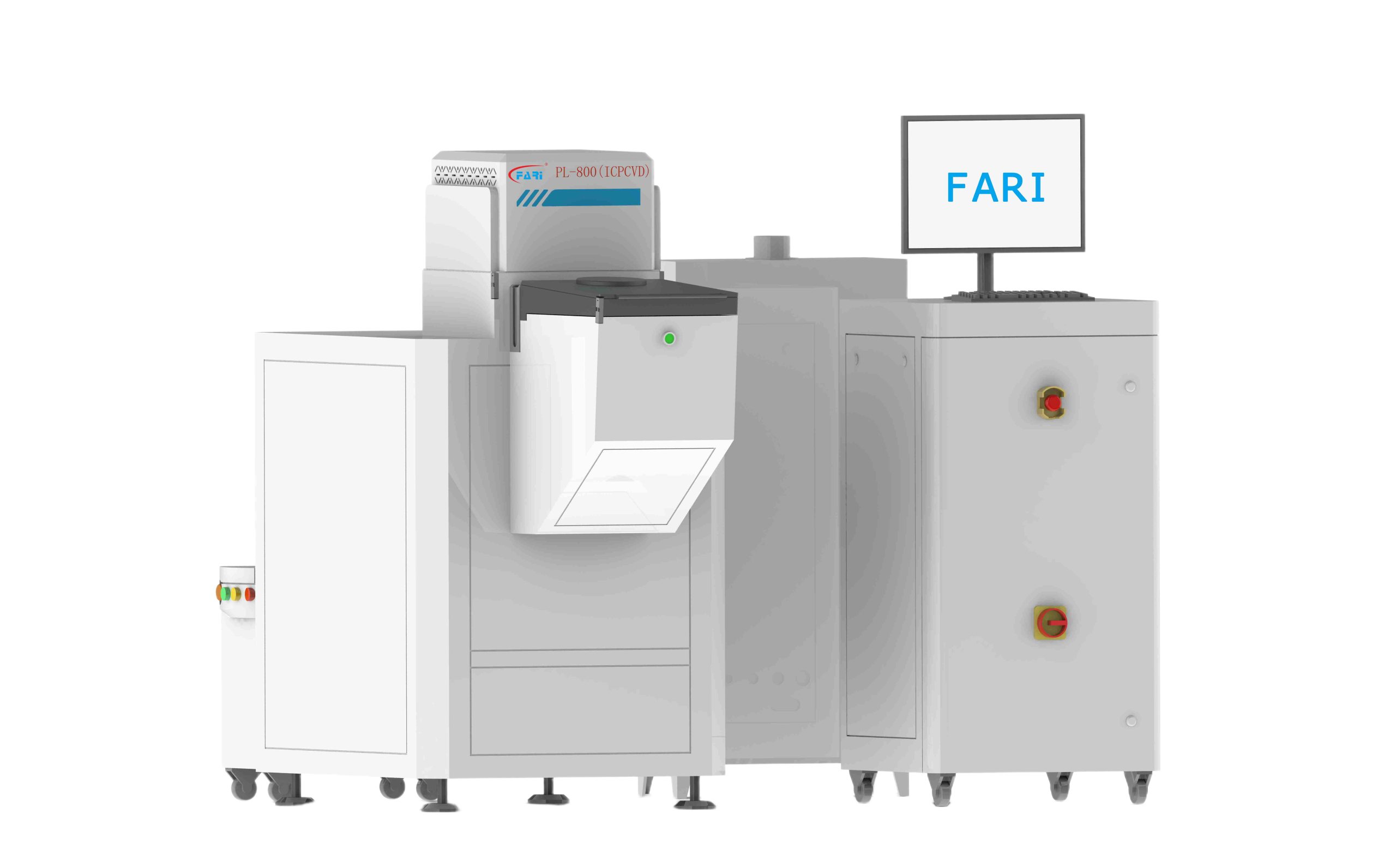
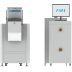
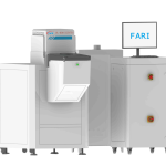
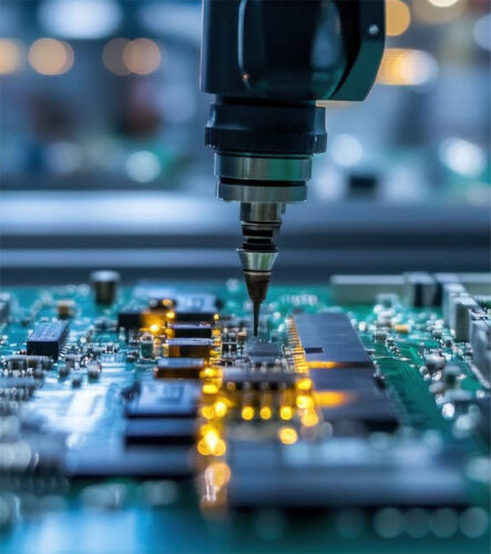
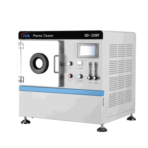
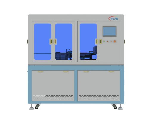
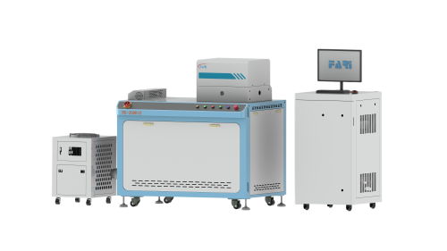
High-density ICP-CVD dual-chamber deposition system designed for SiN, SiO₂ and a-Si thin-film growth. The platform supports uniform and repeatable deposition for semiconductor, photovoltaic, and advanced materials manufacturing.
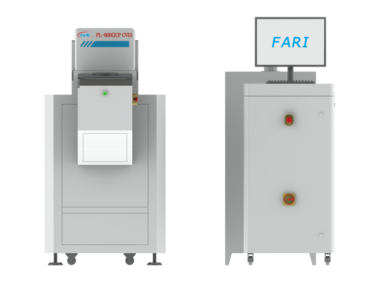
| System Type | Inductively Coupled Plasma Chemical Vapor Deposition (ICP-CVD) |
| Configuration | Dual-chamber design for parallel processing and higher throughput |
| Target Films | Silicon nitride (SiN), silicon dioxide (SiO2), amorphous silicon (a-Si) and composite deposits |
| Main Components | Reaction chambers, vacuum system, gas delivery system, RF power supply, and integrated control system |
| Plasma Source | Inductive RF excitation producing high-density plasma and abundant reactive species |
| Primary Functions | Thin-film deposition and composite material growth through controlled plasma-assisted chemical vapor deposition processes. |


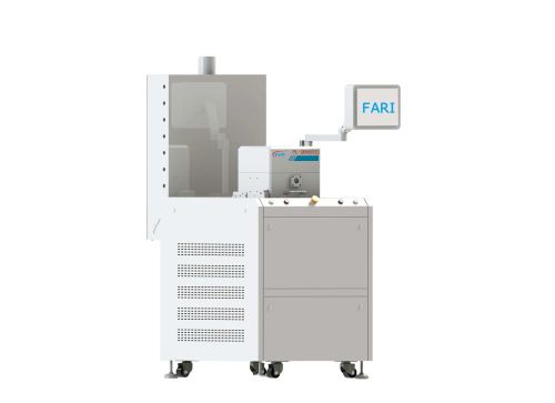
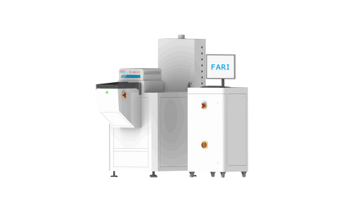
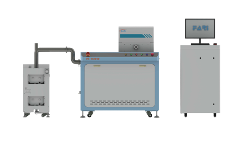
Process gas is energized and converted into a reactive plasma containing ions, electrons, and radicals.

Energetic plasma species interact with surface molecules and contaminants under controlled vacuum conditions.

Reactive ions and radicals break down organic residues and surface contaminants through controlled chemical reactions.

The reaction products are converted into volatile compounds and enter the gas phase.

Gaseous by-products desorb from the surface and are evacuated, leaving a clean, activated material surface.

English

Japanese

Korean
Rogatus ad ultimum admissusque in consistorium ambage nulla praegressa inconsiderate