Semiconductor & Electronics

Plasma Treatment for Semiconductor & Electronics

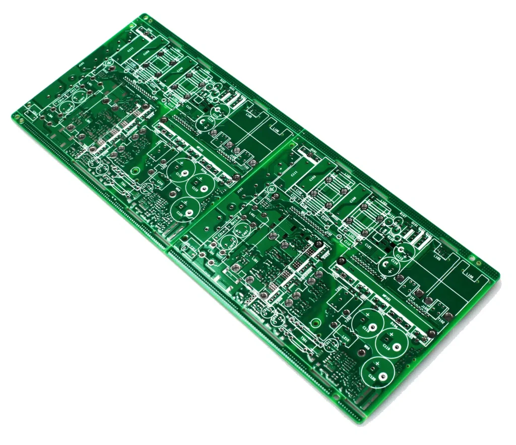
Plasma treatment for semiconductor packaging and PCB assembly replaces solvent cleaning with a dry, ionized-gas step.

Why PCB Makers Add Plasma Cleaning

Most PCB lines run aqueous processes, so flux, mold release, and handling residues carry over from step to step. That film later shows up as coating that beads, wire bonds that pull off pads, or underfill voids. A plasma step before coating, bonding, or encapsulation strips it with ionized gas, not solvent.

Applications

PCB & Electronics Applications We Support

  • Ashing and Descum
  • Wafer Surface Activation
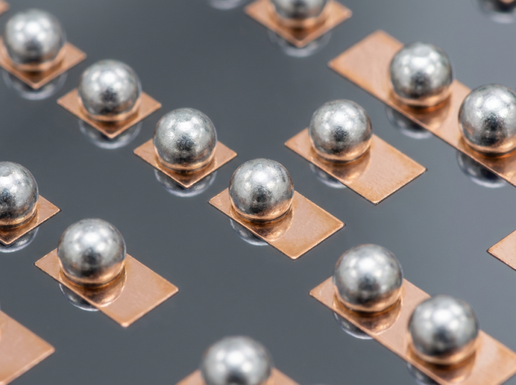
  • Bump and Bond Cleaning
Vacuum, Atmospheric & Inline

Equipment Options for PCB Plasma Cleaning

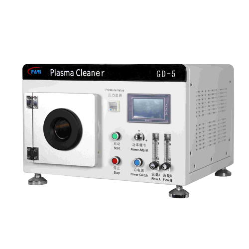
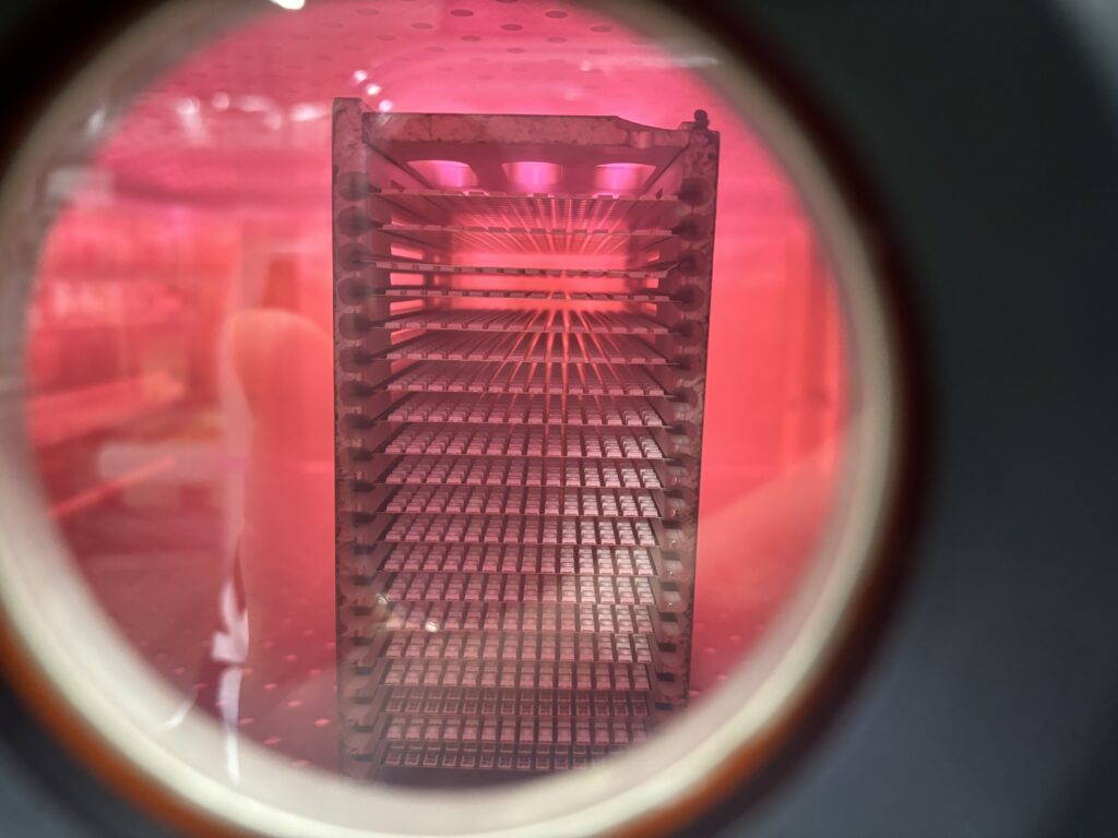
Vacuum plasma systems process boards in a sealed chamber for the most uniform result across a mixed batch. Vacuum Plasma Treatment Explained Inline Plasma Cleaner: Advantages, Limitations & When to Use

  • Sealed Vacuum Batch Chamber

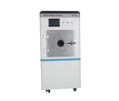
    • GD-30 handles qualification runs and small board lots at 30 Pa base vacuum.
    • GD-600 takes full panel batches in a 600 L sealed vacuum chamber.
    • RD-200 rotates loose connectors and components in a 200 L rotary vacuum drum cleaner with 1–5 kW adjustable power and 2 channels with MFC.
    • Gas mix and power are set per recipe.
  • Atmospheric & Inline Plasma Systems

    • Atmospheric and inline plasma systems run at ambient pressure and integrate directly into a conveyorized assembly line, so boards move through in seconds under the plasma head.
    • There is no vacuum cycle or batch loading, which keeps throughput high for continuous production.
    • The trade-off is less depth of penetration into enclosed cavities than a sealed chamber offers, so deep recesses may need vacuum treatment instead.
    • Inline systems run at ambient pressure on a conveyorized line.
  • Wafer-Level Plasma Etch & Ashing

    • Wafer-level plasma etch and ashing is a different process built for front-end fab lines, running at the die and wafer scale.
    • Wafer-level etch and ashing is a different, front-end fab process.
    • Wafer-level etch and ashing therefore belongs to front-end fab rather than board-level assembly.
    • For board-level work, the vacuum, atmospheric and inline formats above are the relevant options.

Built-to-Spec: Customization for PCB & Assembly Lines

Board sizes, fixture trays, and panel layouts vary line to line, so chamber dimensions, tray and fixture configuration, and automation interfaces are configured to match your assembly process rather than sold as a single fixed unit. Plasma System Customization details what's configurable on a per-order build.

QUALITY CONTROL

Quality Control Before Shipment

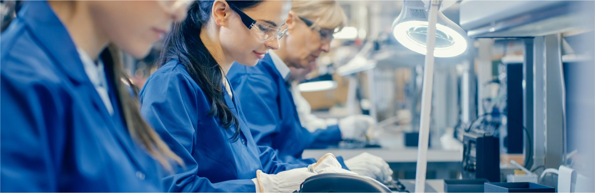
Every unit undergoes visual, electrical, and functional inspection before it leaves the factory, with power output, gas flow, and plasma parameters calibrated and recorded against target values.

  • Full Inspection

    Visual, electrical, and functional inspection on every unit before shipment.

  • Calibrated

    Power output, gas flow, and plasma parameters calibrated and recorded.

  • Traceability

    Serial-numbered units with test data kept for traceability.

  • Clean Assembly

    Assembly in a controlled environment keeps chamber contamination out.

  • Run Tested

    Continuous operation testing prior to shipment, not just a power-on check.

in-house

Why Source PCB Plasma Cleaning Equipment From Fari

Fari has manufactured vacuum and atmospheric plasma equipment since 2011 as a direct manufacturer, keeping design, production, and quality control in-house rather than through a trading intermediary. A plasma treatment for electronics case study documents a scrap-rate reduction achieved after adding a plasma step on a consumer electronics assembly line.

That in-house structure also supports OEM/ODM work: a chamber sized for your board panel is a standard part of how the equipment is built, not a special favor.
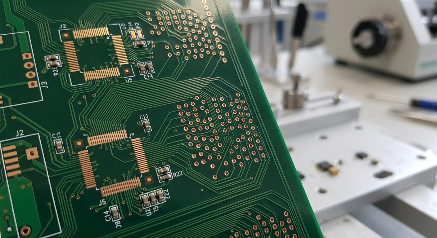
Plasma cleaners overcome this challenge by using high-speed, high-energy plasma to chemically and physically modify the surface. This process optimizes the material's surface, creating an active layer that is essential for successful subsequent operations like printing, bonding, and coating.
Request a Quote for PCB Plasma Cleaning

Sourcing a plasma cleaner for a PCB line covers evaluation, production, shipping, and after-sales support. Contact us with your board dimensions and process step.
FAQS

Frequently Asked Questions

What is PCB plasma cleaning?
It is a dry surface-preparation step that uses ionized gas, typically oxygen or argon, to strip flux, mold release, and organic residue from a board surface before coating or bonding. It runs in a sealed vacuum chamber ahead of a batch process, or inline through an atmospheric unit positioned ahead of the coating or bonding station.
Will plasma cleaning damage sensitive components?
Plasma cleaning is a non-contact, low-thermal process; power and exposure time are recipe-tuned per board so it strips organic residue without lifting solder mask, degrading solder joints, or heating components enough to stress fine-pitch parts. Recipe tuning is still needed per board design before production volume.
How long does plasma cleaning last?
Surface activation fades over time as the board re-contaminates from handling or ambient exposure, so most lines target treating within a few hours of the plasma step, ideally within the same shift, rather than holding treated boards overnight before coating or bonding.
How long does a plasma cleaning cycle take?
A vacuum batch cycle, including load, pump-down, treatment, and vent, typically runs several minutes per load. Inline atmospheric systems move boards through in seconds as they pass under the plasma head on the conveyor, matching line speed rather than adding a separate batch step.
Explore

Explore More Applications

More Applications