


Plastics & Rubber
Plasma treatment increases surface energy, improving adhesion for printing, coating, bonding, and overmolding on low-wettability plastics and elastomers.

Deliver ultra-clean, high-energy surfaces for solar cells, optical components, lenses, and precision coatings, boosting durability and conversion efficiency.
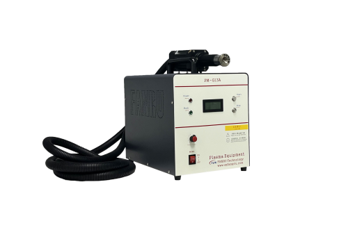
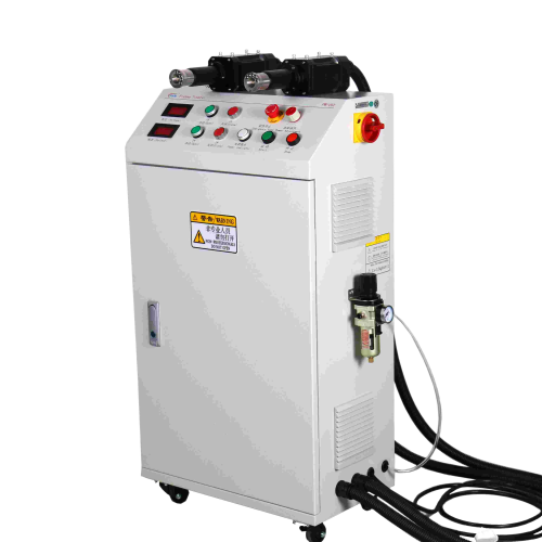
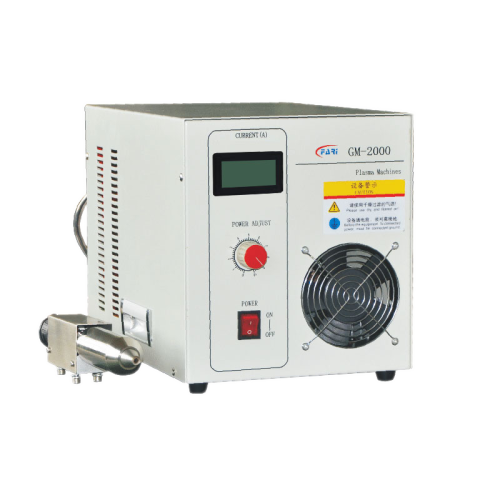
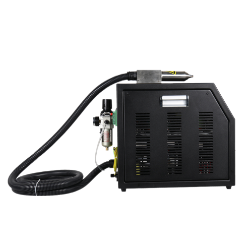
Fari Plasma's plasma cleaning and treatment solutions provide controlled surface activation, contamination removal, and adhesion enhancement for energy and optics components. Applications include solar cell preparation, OLED and display pre-treatment, precision optics cleaning, and fiber‑optic bonding using benchtop plasma cleaners, inline treatment systems, and semiconductor plasma equipment.

Process stability, repeatability, and gas-chemistry selection are critical; oxygen and argon plasmas are used for ashing and cleaning, while tailored chemistries enable functionalization and coating adhesion. Our treatment systems support roll-to-roll and batch production, and semiconductor plasma equipment delivers the sub-micron precision required for descum and lithography-related processes.
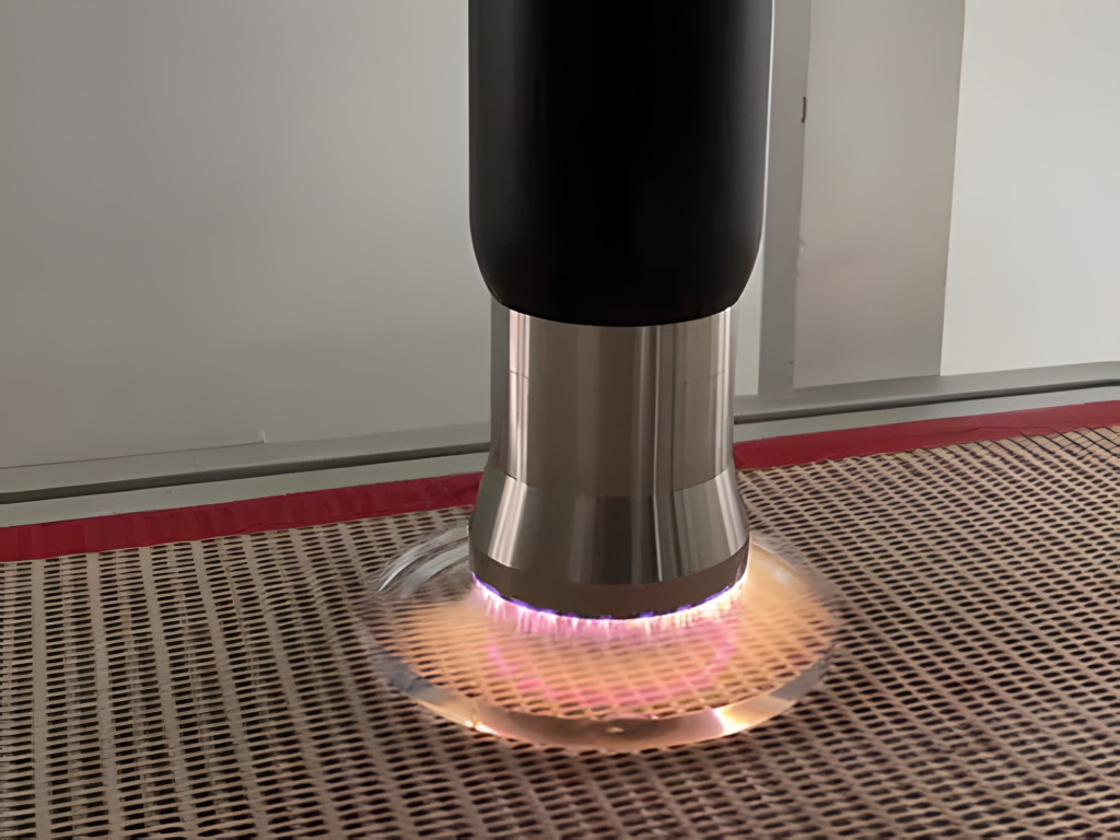

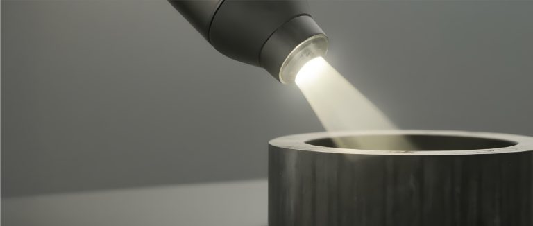
Controlled plasma chemistries activate surfaces to improve wetting and adhesion for coatings and adhesives.

Gentle, low-temperature plasmas process heat-sensitive substrates without thermal damage.

Roll-to-roll and conveyor systems scale plasma treatment from prototypes to high-volume manufacturing.

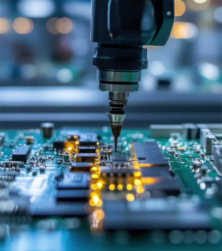
High-uniformity plasma modules provide repeatable descum, ashing, and micro-cleaning for fabs.


Fari Plasma combines engineering expertise and process control to deliver reliable plasma surface solutions for energy and optics manufacturing.


We deliver controlled plasma activation for optics and energy components, improving wetting and adhesion for coatings, films, and functional layers.

Low-temperature plasma treats heat-sensitive substrates without thermal damage, making it ideal for optics, displays, and energy materials.

High-uniformity plasma modules support descum, ashing, and micro-cleaning with repeatable results for semiconductor and precision optics processes.

Inline and roll-to-roll plasma systems scale surface treatment from R&D to high-volume energy and optics manufacturing.


English

Japanese

Korean
Rogatus ad ultimum admissusque in consistorium ambage nulla praegressa inconsiderate