

Can you think of a material that is one atom thick and at the same time stronger than steel, better at conducting electricity than copper, and deformable without breaking?
This is absolute wonder material! This is graphene. It has excellent electrical, mechanical, and thermal properties and is best for cutting-edge applications, such as smartphones and electronic devices.
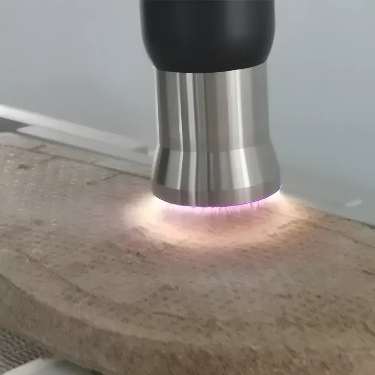
However, graphene is susceptible to surface contamination and defects. By solving these issues, plasma treatment improves graphene’s conductivity without compromising its structure.
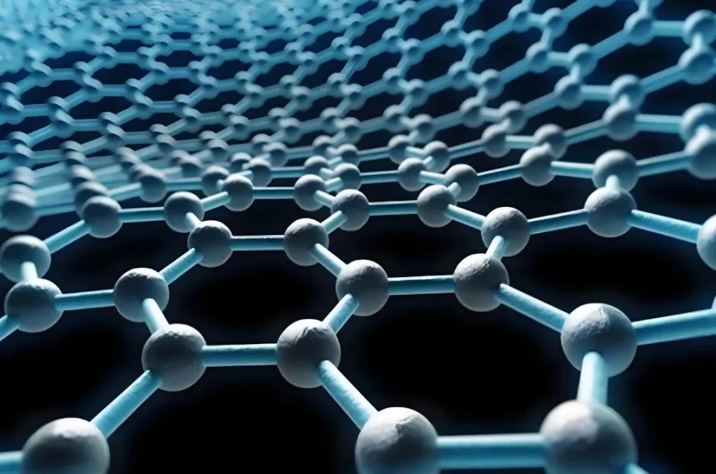
A wonder material in science and technology is known as graphene. It’s made of carbon atoms in one layer in a honeycomb pattern. This unique structure gives graphene extraordinary properties:
There are multiple variables including:
During processing, non-conductive functional groups can also stick to its surface, degrading its performance.
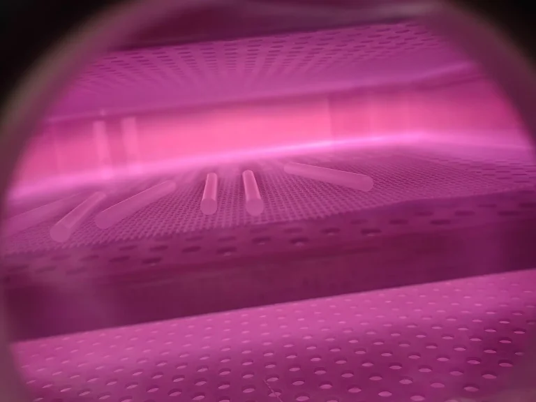
Plasma treatment is a graphene spa day. It’s a precise, non-destructive method that:
Graphene only ‘shines’ on demanding, high-tech applications and achieves its potential through plasma treatment.
Imagine trying to sip water through a blocked straw—that’s what happens to graphene when surface contaminants are present. These impurities, such as organic residues or manufacturing remnants, hinder the smooth movement of electrons.
Plasma treatment acts like a powerful purifier, effectively removing these obstacles. The result? It cleanses the graphene thoroughly, preserving its intricate structure and optimizing its performance.
Plasma treatment is not only restricted to cleaning. The seminal flow of electricity mucks up missing atoms or structural gaps. Plasma treatment acts as the repair crew by reinforcing the connections between graphene layers, thus increasing performance.
This is where plasma treatment gets interesting. Like a magnet, it can ‘stick’ a defined group of chemical atoms (oxygen or hydrogen) onto or off graphene’s surface. The flexibility of customizing graphene makes it possible to tune properties to enhance conductivity and flexibility.

Imagine if electrons traveled on a highway: that’s our graphene. Electrons shoot through quickly when they are clean and defect-free. The plasma treatment overcomes roadblocks, such as contaminants, by fixing the structural defects to provide an easier path through which electrons can flow.
It’s fantastic that plasma treatment is the only method that is so gentle. Other methods may damage graphene’s delicate atomic structure.
Here’s another win for plasma treatment: It’s scalable and sustainable. It’s a ‘dry’ process, so they don’t use harsh chemicals, which is good for the environment. Our design ensures scalability for extensive applications, making it perfect for integrating thousands of graphene sheets into industrial devices.
Plasma-treated graphene has another hidden talent; It is better bonded to other materials. Because of plasma treatment, graphene will sit like a glove in a battery, solar cell, or touchscreen. Therefore, the final device should function better and last longer.
Graphene treated with plasma has become a high-performing, versatile material for many of today’s advanced applications.
Imagine a smartphone that you can fold away or a fitness tracker you can wrap around your wrist. These materials need to be highly conductive, even when bent or twisted, and because of that, making these devices will be challenging.
Plasma-treated graphene steps up to challenge it. This ensures that conductivity will remain stable and is fit for foldable screens, wearable tech, and flexible circuits.
Batteries and supercapacitors are all about efficiency. Plasma-treated graphene improves electron flow, enabling much faster graphene charging and better energy storage.
This is a game changer for technologies such as electric cars and portable devices, where strong-performance batteries play a critical role.
Sensors must combine precision with speed. Graphene sensors enhanced by plasma treatment are capable of identifying chemicals, biological substances, and environmental shifts.
Touchscreens, OLED screens, and solar panels are fancy. These all require see-through conductive material. These cutting-edge applications require something conductive and optically transparent, and graphene treated with plasma satisfies both areas and is the best bet.
Plasma treatment requires a customized approach, much like crafting a recipe where every ingredient plays a crucial role. Firstly, there is gas composition. The type of gas – argon, oxygen, or even hydrogen – modifies how the surface of the graphene is changed. For example, oxygen introduces a functional group to a compound; and argon removes impurities.
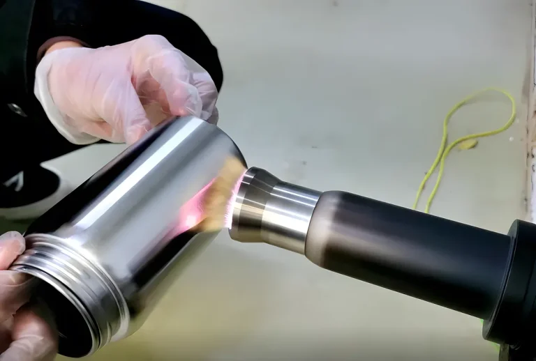
Both power and duration need to be precisely calibrated. In plasma treatment, delicate graphene can be easily damaged by excessive energy or prolonged exposure. Maintaining uniform pressure and temperature in the chamber is essential.
Raman spectroscopy is the health check of graphene: It looks at the structure and sees if any more defects are left. If we measure electrical conductivity, we can measure something like sheet resistance or electron mobility, and we know how much better it gets. These tests assure us that graphene can be used for high-performance applications.
Imagine cleaning a fragile piece of jewelry too vigorously—it could easily get damaged! The idea is the same in plasma treatment. However, excessive amounts of this treatment are bad for graphene, creating new defects or over functionalizing the surface. In fact, it can even decrease conductivity, which is antithetical to treatment. But the key is balancing this all out correctly to avoid these pitfalls.
Not all graphene is equal. This plasma treatment approach is not one size fits all. Due to the differences in properties between different types of graphene, their treatment requires improving their features without causing damage, so each type requires different settings for its treatment.
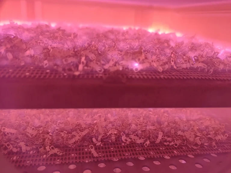
Plasma treatment must be integrated in a way that is useful at a large scale and still fits within a reasonable amount of time without too much stoppage or difficulty. Whether it is for electronics, sensors, or energy storage devices, the process needs to be both efficient and compatible with industrial setups.
Plasma equipment isn’t cheap, but the initial investment usually pays off. Enhanced graphene performance leads to more efficient devices, more energy savings, and less waste—and that’s simply enough reason for an industry that wants to innovate to spend.
Supercapacitors are the sprinters of the supercapacitor world – they charge and discharge fast. It is essential to be highly conductive so that they can store and release energy efficiently. Researchers say plasma-treated graphene dramatically increases energy storage capacity. Instead, they make supercapacitors less capricious but more powerful — thus perfect for electric vehicles and renewable energy systems.
Did you ever think of bendable fitness trackers or foldable smartphones? However, these gadgets need circuits that can flex repeatedly and remain functional. This is a game changer, plasma-treated graphene.
The material conductivity increases, allowing these flexible devices to maintain expected performance even when repeatedly folded or twisted.
Touchscreens, solar panels, and OLED displays require conductive, see-through materials. Plasma treatment improves the performance of graphene films, boosting touch sensitivity and display brightness in devices.
Imagine adding just the right amount of spice to those farmer’s market peppers you’re grilling. Scientists are using plasma treatment to introduce oxygen or nitrogen as specific ‘sub functional’ groups on graphene.
What if one combines graphene with other two-dimensional materials to make composites? When graphene is modified with plasma, mixing this material with others like boron nitride or molybdenum disulfide is possible, creating still more efficient and versatile hybrids.
AI is now making plasma treatment brighter. With AI-driven systems, you can view the process in real time and adjust process parameters to ensure consistently high quality and efficiency.
With fewer errors and increased speed compared to before, players can be produced rapidly, making the process perfect for large-scale industrial applications.
This is a green alternative to the evolutive toxic methods of industries. It works against waste and harsh chemicals and perfectly fits the drive to manufacture sustainably.
Plasma treatment of graphene is changing the way people use it. This treatment is not conductive but helps improve graphene’s conductivity from bendable electronics like foldable phones to very efficient energy storage systems like batteries and supercapacitors.
The FariPlasma provides high quality plasma treatment with long-term benefits. The value of these plasma-treated graphene is that the upfront costs far outweigh how much better, much longer it lasts, and how seamlessly it goes into cutting-edge devices.
What truly captivates me is the ongoing and future research within this discipline. We’re using plasma treatment more smartly and efficiently to figure out the potential of graphene.


English

Japanese

Korean
Rogatus ad ultimum admissusque in consistorium ambage nulla praegressa inconsiderate