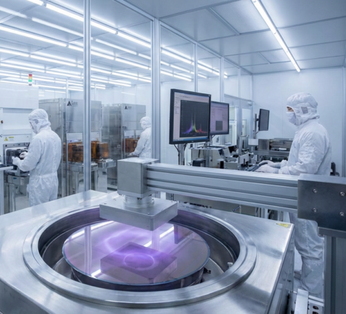
In semiconductor manufacturing, PCB fabrication, and advanced micromachining, precision is everything. One of the most critical processes in these industries is plasma ashing, a technique that removes unwanted photoresist and organic materials with remarkable precision and efficiency.
Plasma ashing, also known as plasma stripping or photoresist removal, is a dry etching process that uses low-temperature plasma to remove photoresist and other organic materials from semiconductor wafers, PCBs, and other substrates. Unlike wet chemical stripping methods, plasma ashing offers superior control, minimal substrate damage, and environmentally friendly operation.
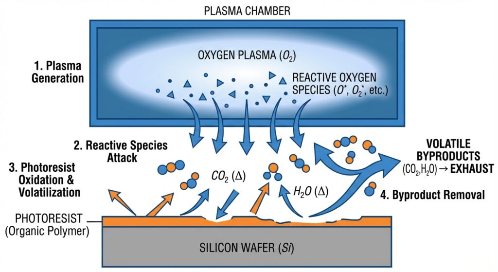
The term "ashing" comes from the process's ability to reduce organic polymers to ash-like residue. When photoresist—a light-sensitive polymer used in lithography—has served its purpose in pattern definition, it must be removed cleanly and completely before the next manufacturing step. Plasma ashing accomplishes this with elegance and precision.
Before diving into the mechanics, let's understand why this process matters so much in modern manufacturing:
Pattern Definition: Photoresist is applied to wafers and exposed through masks to define circuit patterns. Once the underlying material (metal, dielectric, or semiconductor) has been processed, the photoresist becomes obsolete.
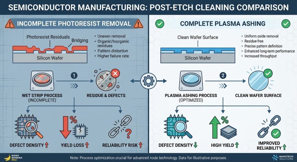
Surface Cleanliness: Residual photoresist compromises device performance, yield, and reliability. Even microscopic traces can cause defects in subsequent processing steps.
Yield and Cost: Incomplete photoresist removal leads to device failures, reduced yields, and increased manufacturing costs. The ability to remove 100% of resist ensures maximum return on investment.
Process Integrity: In multi-layer semiconductor fabrication, each layer must be completely clean before the next layer is processed. Plasma ashing ensures this integrity without chemical residues that wet stripping leaves behind.
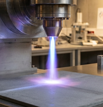
First, let's demystify plasma itself. Plasma is often called the "fourth state of matter"—beyond solid, liquid, and gas. It consists of ionized gas containing electrons, ions, and neutral atoms in a quasi-neutral mixture. When electrical energy is applied to a gas at low pressure, it becomes ionized and enters this plasma state.
The plasma ashing process works through several complementary mechanisms:
1. Chemical Oxidation
In a typical plasma ashing system using oxygen-based plasma (O₂ plasma), the following occurs:
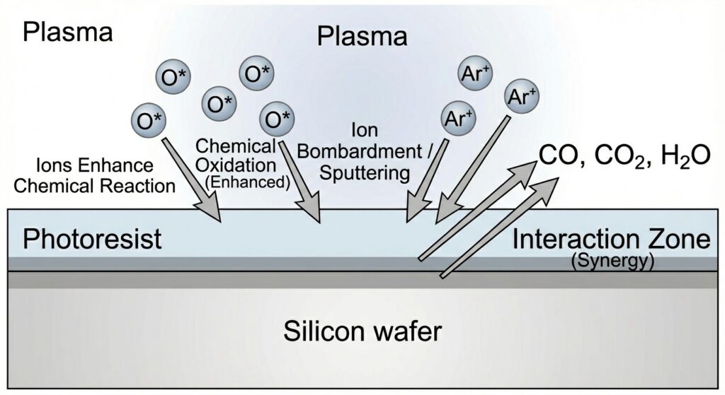
2. Physical Sputtering
While chemical oxidation is the primary mechanism, physical sputtering contributes to material removal:
3. Ion-Enhanced Etching
Ion-enhanced etching combines both chemical and physical mechanisms:
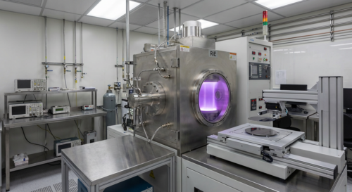
A typical plasma ashing system consists of:
| Component | Function |
|---|---|
| Vacuum Chamber | Contains the plasma and isolates the process from atmospheric interference |
| Gas Supply System | Delivers oxygen or other process gases with precise flow control |
| RF Power Source | Generates the electromagnetic energy that ionizes the gas (typically 13.56 MHz) |
| Electrode Configuration | Creates the electric field distribution (parallel plate, capacitive, or inductive designs) |
| Temperature Control | Maintains substrate temperature, typically 20-200°C |
| Exhaust System | Evacuates gaseous byproducts safely and efficiently |
| Control System | Monitors and adjusts process parameters in real-time |
Successful plasma ashing depends on precise control of several variables:
Pressure: Typically 0.1 to 1 Torr (roughly 133 Pa to 1333 Pa). Lower pressure increases the mean free path of reactive species, favoring chemical etching. Higher pressure increases collision rates, affecting etch uniformity.
Power: Radio-frequency power (measured in Watts) controls plasma density and ion energy. Higher power accelerates removal but increases the risk of substrate damage and resist notching (undercutting at resist edges).
Gas Flow: Oxygen flow rate (measured in sccm—standard cubic centimeters per minute) determines the supply of reactive species. Optimal flow prevents both oxygen depletion and excessive pressure buildup.
Temperature: Substrate temperature affects reaction kinetics. Room temperature to 150°C is typical, with higher temperatures accelerating ashing but potentially damaging temperature-sensitive substrates.
Time: Process duration depends on resist thickness (typically 0.5 to 3 micrometers) and process conditions. Overexposure can damage underlying layers.
While wet chemical methods (sulfuric acid/hydrogen peroxide, for instance) have been used historically, plasma ashing offers compelling advantages:
Plasma ashing serves diverse manufacturing sectors:
Semiconductor Manufacturing: Removing photoresist in wafer fabrication, especially in advanced nodes with tight tolerances.
PCB Fabrication: Cleaning circuit board substrates between lithographic steps.
MEMS and Advanced Micromachining: Processing delicate microstructures where wet chemicals pose contamination risks.
LED Manufacturing: Preparing sapphire and GaN substrates for subsequent processing.
Optical Components: Cleaning precision optical surfaces without contamination.
Plasma ashing represents a quantum leap in manufacturing precision and efficiency. By harnessing the unique properties of ionized gas, manufacturers can achieve complete photoresist removal while protecting underlying structures and maintaining environmental responsibility. At Fari Plasma, our advanced plasma treatment systems deliver the reliability, precision, and performance that modern manufacturing demands.
Whether you're scaling semiconductor production, advancing PCB complexity, or pushing the boundaries of micromachining, understanding plasma ashing is essential to optimizing your process and maximizing your manufacturing potential. The future of precision manufacturing runs on plasma.

English

Japanese

Korean
Rogatus ad ultimum admissusque in consistorium ambage nulla praegressa inconsiderate