Plasma etching has become an indispensable technology in modern manufacturing, particularly in the semiconductor, microelectronics, and advanced materials industries.
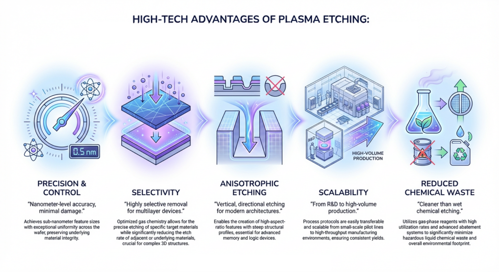
Plasma etching is a process that uses ionized gas (plasma) to remove material from a solid surface with exceptional precision and control. Unlike traditional chemical etching or mechanical abrasion, plasma etching operates at the molecular level, allowing manufacturers to create intricate patterns and features with nanometer-level accuracy.
The term "etching" refers to the selective removal of material, while "plasma" describes the ionized state of gas used in the process. When gas is energized through electrical discharge, it transforms into plasma—a fourth state of matter containing ions, electrons, and neutral atoms. This highly reactive state makes plasma ideal for controlled material removal in manufacturing.
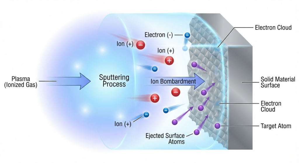
The foundation of plasma etching begins with ionization. When electrical energy is applied to a gas at low pressure, electrons are stripped from gas atoms, creating ions and free electrons. This process transforms ordinary gas into an energized plasma state capable of interacting with solid materials in controlled ways.
At Fari Plasma, our systems generate plasma using various methods:

Plasma etching operates through two primary mechanisms:
Physical Sputtering: High-energy ions bombard the material surface, physically dislodging atoms through kinetic energy transfer. This is a direct, momentum-based removal process.
Chemical Reaction: Reactive species generated in the plasma chemically react with the target material, forming volatile compounds that escape as gases. This chemical process is often more selective and controllable than pure physical sputtering.
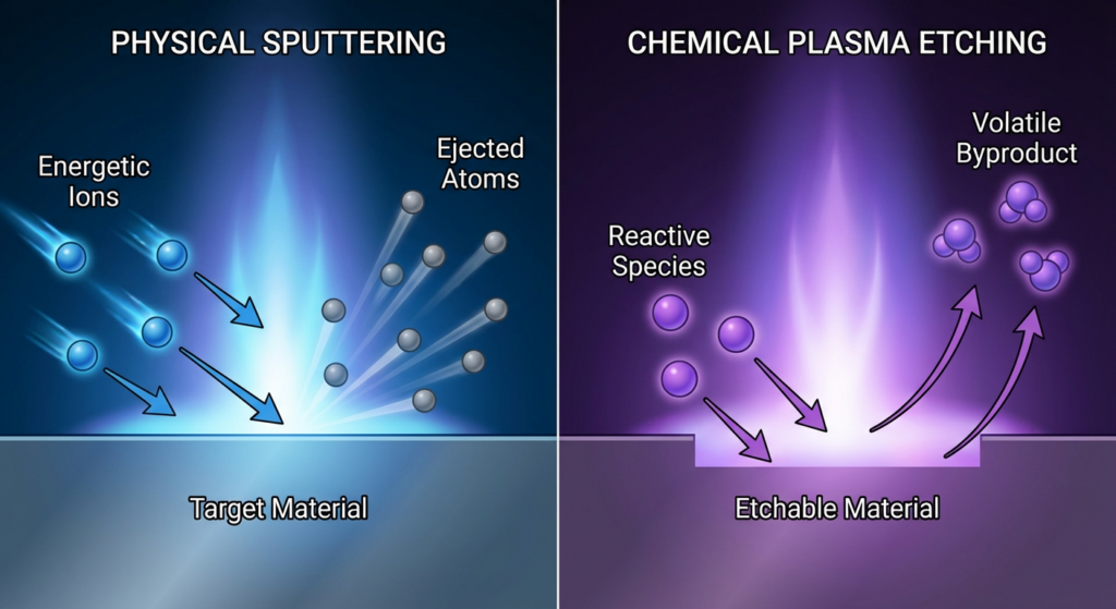
Most practical plasma etching processes combine both mechanisms, creating a hybrid approach that offers the best of both worlds: precision from physical sputtering and selectivity from chemical reactions.
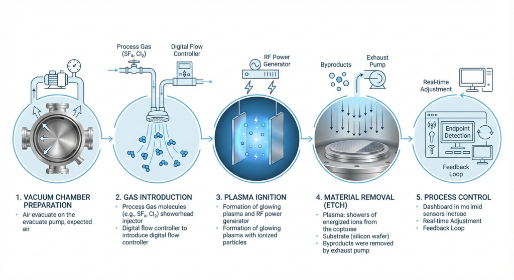
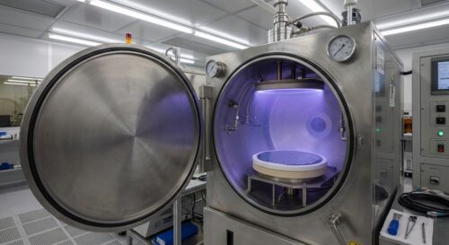
The etching process begins by placing the substrate (the material to be etched) inside a vacuum chamber. The chamber is evacuated to low pressure—typically between 0.1 and 10 Pa—to ensure optimal plasma formation and control.
Specialized etching gases are introduced into the chamber. Common gases include:
The gas flow rate and pressure are carefully controlled to maintain optimal process conditions.
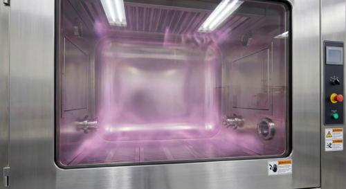
Electrical energy is applied to the chamber, ionizing the gas and creating plasma. The energy level, frequency, and power are precisely controlled to achieve the desired plasma characteristics.
Once plasma is established, reactive species (ions, radicals, and excited atoms) interact with the substrate surface. Through the combined physical and chemical mechanisms described earlier, material is selectively removed according to the pattern defined by protective masks or resist structures.
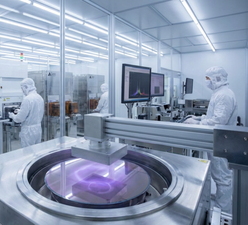
Throughout the etching process, parameters such as power, pressure, temperature, and gas flow are continuously monitored and adjusted to ensure precision. When the desired etch depth is achieved, the power is turned off, plasma disappears, and the process terminates.
Different plasma etching techniques are optimized for specific applications:
RIE combines ion bombardment with chemical reactivity, offering excellent directionality and precision. This is the most widely used plasma etching technique in semiconductor manufacturing.
ICP systems use inductive coupling to generate high-density plasma, enabling faster etch rates with superior control. This technology is essential for advanced semiconductor patterning.
This variant uses plasma to enhance chemical reactions at lower temperatures, making it ideal for temperature-sensitive applications.
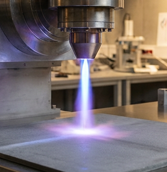
Fari Plasma specializes in atmospheric pressure plasma technologies that eliminate the need for vacuum chambers, offering cost-effective solutions for many industrial applications.
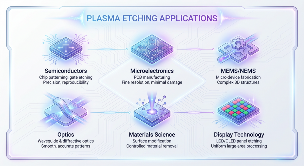
Plasma etching technology finds applications across numerous industries:
Plasma etching represents one of the most powerful technologies in modern manufacturing. By harnessing the unique properties of ionized gas, manufacturers can achieve precision, control, and reproducibility impossible with conventional methods. Whether creating cutting-edge semiconductor devices, advanced medical components, or innovative materials, plasma etching makes it possible.
At Fari Plasma, we're committed to advancing plasma technology, helping manufacturers worldwide realize their most ambitious production goals. As your partner in plasma innovation, we provide the systems, expertise, and support needed to master this transformative technology and stay competitive in rapidly evolving markets.

English

Japanese

Korean
Rogatus ad ultimum admissusque in consistorium ambage nulla praegressa inconsiderate