Plasma resist removal — oxygen plasma ashing — clears photoresist from wafers, PCBs, and optical substrates after lithography or etch, with no wet chemical strip and no rinse step. If a line needs resist cleared completely before the next coating, bonding, or deposition step, talk to our team about a system spec.
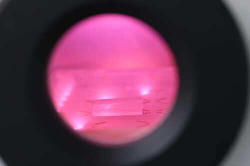
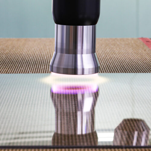
Oxygen gas ionized inside the chamber breaks into reactive oxygen radicals and ions. Those species attack the organic polymer chains in the photoresist and convert the resist into volatile byproducts — mainly CO₂ and water vapor — that the vacuum system pumps out of the chamber. Nothing is dissolved, sprayed, or scrubbed off the substrate; the resist reacts away until the surface underneath is bare, which is why ashing avoids the chemical residue and disposal cost that come with wet stripping.
Resist removal runs immediately after the step the photoresist was protecting, before the wafer or board moves on:
Resist that survives removal doesn't just look untidy — it shows up downstream as inconsistent adhesion, uneven metal deposition, or bonding failures that are hard to trace back to the ashing step once they surface.
The three chamber types trade speed against damage risk. Downstream (remote) plasma generates the plasma outside the process chamber, so most ions recombine before reaching the wafer — the lowest ion energy of the three, gentlest on sensitive layers, but the slowest resist clearing. ICP (inductively coupled) plasma runs the process inside the chamber at moderate ion energy, clearing resist faster than a downstream setup while still limiting substrate heating. RIE adds physical ion bombardment on top of the chemical reaction: the fastest resist removal of the three, but the same ion energy that speeds up ashing raises the risk of substrate damage and localized heating on temperature-sensitive layers, so RIE cycles need tighter power and time control than a downstream or ICP recipe.
Soft-baked resist reacts fastest, since the polymer hasn't been hardened by additional heat or ion exposure. Hard-baked resist — cross-linked by a post-develop bake — takes longer to break down under the same plasma conditions. Resist that's been ion-implanted through develops a hardened, ion-modified crust on its surface that has to break down before the bulk resist clears, extending the cycle. Post-etch polymer residue, a mix of resist and etch byproducts rather than plain resist, typically needs a higher oxygen dose than a straightforward resist strip to clear completely.
| System | Removal Mechanism | Control | Best Suited For |
|---|---|---|---|
| GD-20RF Plasma Asher | Downstream oxygen-plasma ashing | PLC + touch screen; automatic/manual modes | A plasma asher for wafers and small-batch photoresist stripping where substrate sensitivity matters more than speed |
| ICP Plasma Residue Removal System | Inductively coupled oxygen plasma | PLC + touch screen; automatic/manual modes | Higher-throughput batch resist and residue clearing |
| SD-300 ICP Photoresist Stripper | ICP resist stripping | PLC + touch screen; automatic/manual modes | Wafer-scale photoresist stripping runs |
| RIE Plasma Resist Stripping System, PE-200 Reactive Ion Etcher, Single-Chamber RIE Etcher | Reactive-ion etch: chemical reaction plus ion bombardment | PLC + touch screen; automatic/manual modes | Hard-baked or post-etch resist that needs faster clearing |
Chamber size, RF power, operating pressure, and wafer-size compatibility are set per configuration rather than fixed across the catalog — Fari's OEM/ODM process confirms these, along with gas channel count, automation interface, and branding, during technical evaluation for the specific resist and substrate involved.
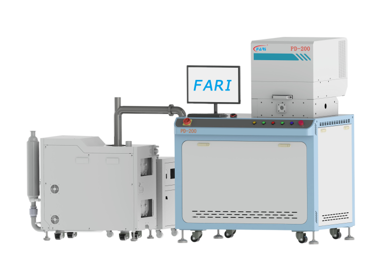
Fari has manufactured plasma equipment directly — not as a trading company — since 2011, running in-house R&D, production, and quality control from a 3,000 m² factory, and holds ISO 9001 certification (since 2021) plus a CE certification history across its vacuum plasma line. Every asher and stripper ships with a factory acceptance test log: power output, gas flow, and plasma parameters calibrated and recorded against that unit's serial number, so a repeat order runs the same recipe the first unit did, not a re-tuned approximation of it. Large stock on catalog configurations supports faster quoting, and reinforced packaging is built for international shipment.
What are the best methods for removing photoresist? Plasma ashing (dry, oxygen-based) and wet chemical stripping are the two main routes. Ashing clears resist completely without liquid waste or rinse steps and holds tighter process control; wet stripping costs less in equipment but carries residue risk and disposal cost on hardened or post-etch resist.
Does acetone remove photoresist? Acetone works on soft, unexposed resist but is inconsistent on resist hardened by etch, implant, or heat exposure — it often leaves a residual film at feature edges that oxygen plasma ashing removes completely.
What is the purpose of oxygen plasma ashing? To convert photoresist into volatile byproducts pumped out of the chamber, clearing the resist layer completely without wet chemicals or the mechanical stress of scrubbing.
Fari's order process runs from technical evaluation through customized production, shipping, and after-sales support. Send the resist type, substrate, and batch size and get a specification back for a suitable asher or ICP/RIE stripping system: request a quote.

English

Spanish
Rogatus ad ultimum admissusque in consistorium ambage nulla praegressa inconsiderate