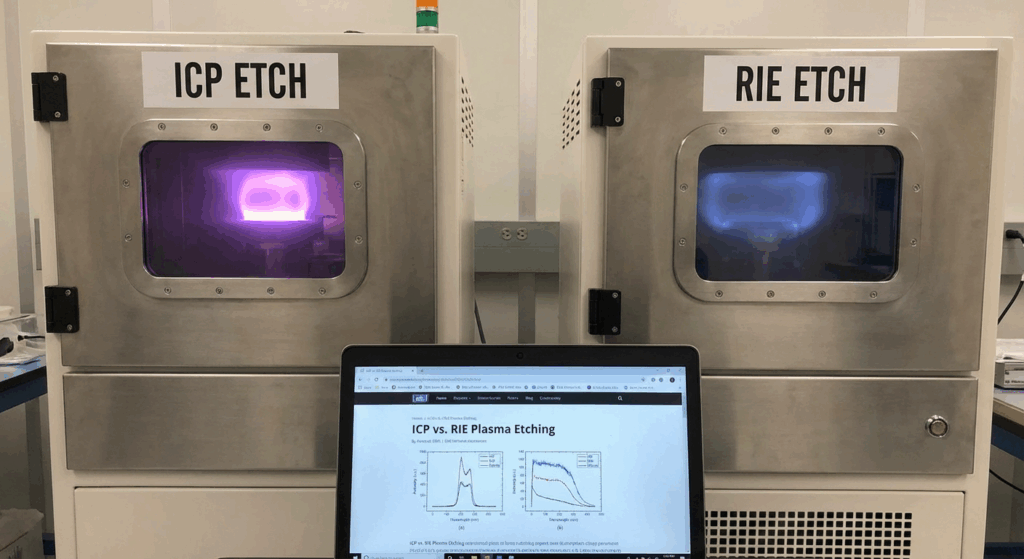
Plasma etching has become an indispensable technology in modern semiconductor manufacturing, materials processing, and surface treatment. Among the various plasma etching techniques, two methods stand out as industry workhorses: Inductively Coupled Plasma (ICP) etching and Reactive Ion Etching (RIE). While both technologies utilize ionized gas to remove material from surfaces, they operate on fundamentally different principles and offer distinct advantages for specific applications. Understanding these differences is crucial for manufacturers and researchers who need to select the right technology for their production requirements.
Before diving into the specifics of ICP and RIE, it's helpful to understand plasma etching as a whole. Plasma etching is a dry etching process that uses ionized gas—plasma—to chemically and physically remove material from a substrate. Unlike wet chemical etching, which uses liquid solutions, plasma etching offers superior precision, consistency, and the ability to create highly directional etch profiles.
The plasma itself is created by applying electromagnetic energy to a gas at low pressure, stripping electrons from gas atoms and creating a mixture of ions, electrons, and neutral radicals. These reactive species interact with the substrate surface, removing material through chemical reactions, physical sputtering, or a combination of both.
RIE has been the backbone of plasma etching technology for decades. This technique applies a radiofrequency (RF) electric field directly to the electrode holding the substrate, creating a self-bias that accelerates ions toward the surface.
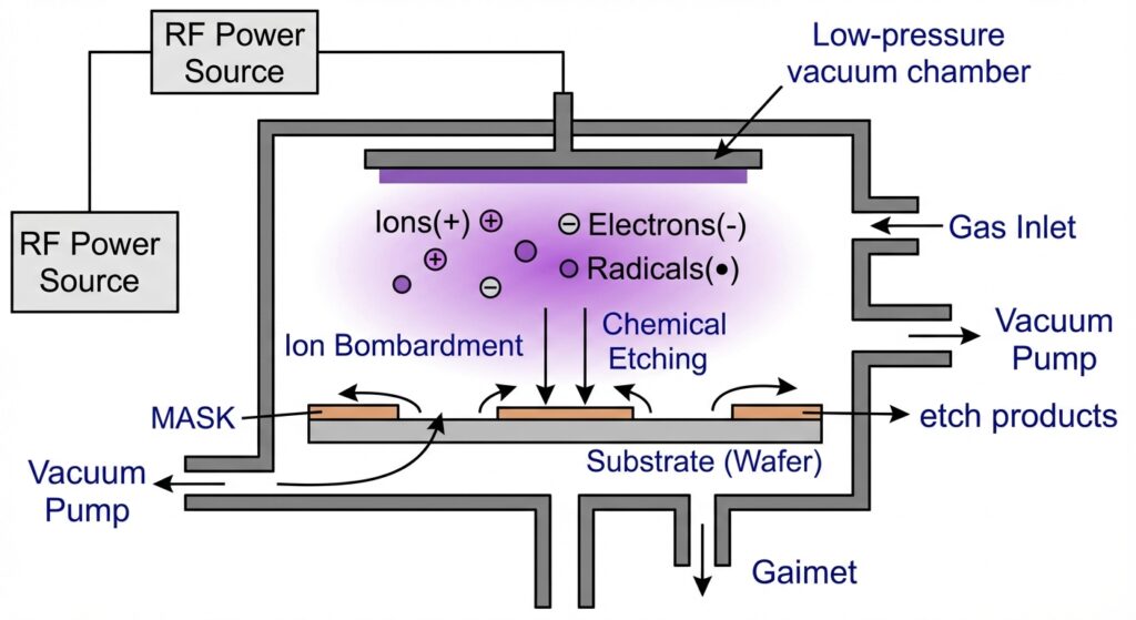
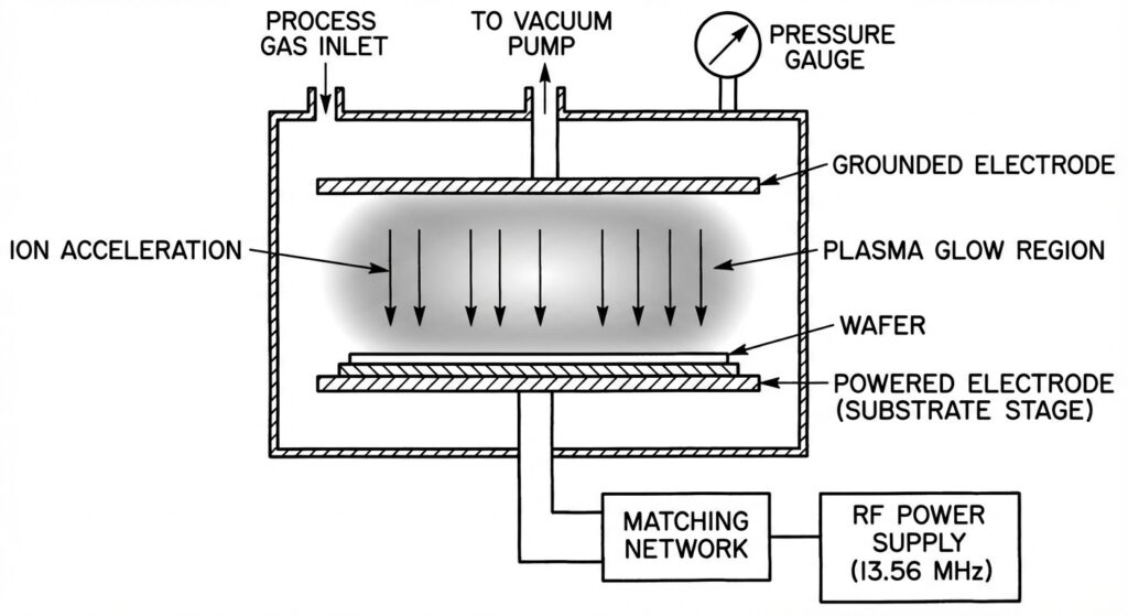
In an RIE system, the plasma is generated between two electrodes in a vacuum chamber. One electrode (the cathode) holds the substrate being etched, while the other (the anode) is grounded. When RF power is applied at 13.56 MHz, a glow discharge is initiated. The key characteristic of RIE is that the same RF field that creates the plasma also accelerates ions directly toward the substrate.
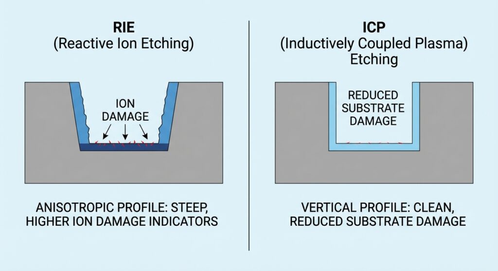
This direct acceleration creates a strong directional component to the etching process. Ions bombard the surface with significant energy, typically in the range of 100-500 eV, enabling highly anisotropic etching profiles. This means material is preferentially removed vertically rather than laterally, resulting in steep-walled features that are essential for modern semiconductor devices.
Simplicity and Cost-Effectiveness: RIE systems are relatively straightforward to design and operate. The single RF source and simple electrode configuration make these systems more affordable than their ICP counterparts.
Excellent Directional Control: The direct ion bombardment provides outstanding anisotropy, making RIE ideal for applications requiring high-aspect-ratio features and minimal undercutting.
Proven Track Record: RIE technology has been extensively developed and refined over the past four decades, with well-established processes for numerous materials.
Compact Design: RIE systems typically require less floor space and infrastructure than ICP systems, making them suitable for facilities with space constraints.
However, RIE does have notable drawbacks. The direct RF field that accelerates ions toward the substrate also tends to generate significant heat and substrate damage through energetic ion bombardment. This bombardment can create lattice defects, alter material properties, and introduce defects that compromise device performance. Additionally, RIE exhibits lower etch rates compared to ICP, which can impact productivity in high-volume manufacturing environments.
The plasma density in RIE is also relatively low, typically in the range of 109 to 1010 cm⁻³, which limits the availability of reactive radicals and restricts etch rate potential.
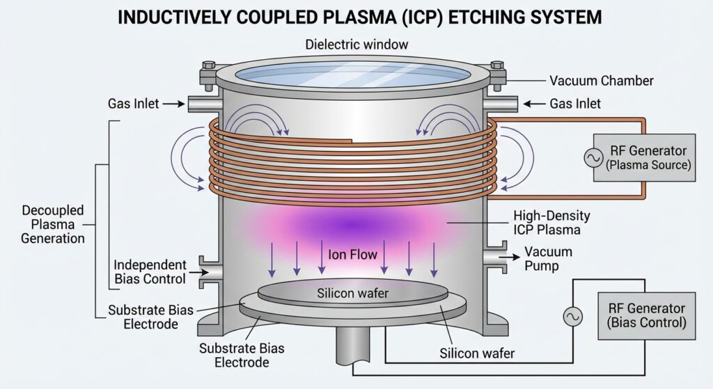
ICP etching represents a more advanced approach to plasma generation and has become increasingly prevalent in semiconductor manufacturing over the past two decades. Rather than directly accelerating ions with the same field that creates the plasma, ICP systems decouple plasma generation from ion acceleration.
In an ICP system, plasma is generated by electromagnetic induction using a coil positioned outside the vacuum chamber. An RF power supply (typically at 13.56 MHz) energizes this coil, inducing a magnetic field that ionizes the process gas through electromagnetic induction. The resulting plasma density is substantially higher than in conventional RIE—often reaching 1011 to 1012 cm⁻³ or even higher.
Once the high-density plasma is created, a separate RF source at the substrate electrode provides the substrate bias. This bias accelerates ions toward the surface, but the separation of plasma generation from ion acceleration allows independent control of both parameters.
Superior Etch Rates: The dramatically higher plasma density in ICP systems translates directly to higher etch rates. Production facilities can achieve 2-10 times faster etching compared to RIE systems for many materials, significantly improving throughput.
Independent Control Parameters: The decoupling of plasma generation from ion acceleration allows operators to optimize etch rate (through coil power) and anisotropy (through bias power) independently. This flexibility enables process optimization for specific applications.
Reduced Substrate Damage: While maintaining directional etching, ICP systems can achieve high etch rates with lower substrate bias voltages. This reduces energetic ion bombardment and associated substrate damage, crucial for advanced devices where defect-free surfaces are essential.
Lower Operating Costs: Higher etch rates mean shorter processing times and reduced operational expenses despite potentially higher equipment capital costs.
Better for Complex Chemistries: The high radical density in ICP systems facilitates more sophisticated chemistry combinations, enabling etching of difficult-to-process materials.
Higher Equipment Cost: ICP systems are more complex and expensive than RIE systems, requiring additional RF sources and induction coils.
Increased Complexity: Operating ICP systems requires more expertise and sophisticated process control. Parameter interactions are more complex than in RIE systems.
Larger Equipment Footprint: ICP systems typically require more space and more complex facility infrastructure.
Potential for Plasma Asymmetry: Large-scale ICP systems can suffer from non-uniform plasma generation, leading to process uniformity challenges across the substrate.
The most fundamental difference between ICP and RIE is plasma density. ICP systems generate densities of 1011 to 1012 cm⁻³, while RIE systems typically produce 109 to 1010 cm⁻³. This tenfold to hundredfold difference has cascading effects on all other parameters.
RIE systems produce ions with more uniform energy distributions due to the direct acceleration by the RF field. ICP systems generate a broader energy distribution, but the key advantage is that most ions are generated before reaching the electrode, allowing lower bias voltages while maintaining directional etching.
For silicon etching with a chlorine/argon chemistry, RIE systems might achieve etch rates of 100-300 nm/minute, while ICP systems typically reach 500-2000 nm/minute or higher. This difference becomes even more pronounced for materials requiring chemically intensive processes.
Both technologies can achieve anisotropic etching, but they approach the problem differently. RIE achieves anisotropy through high ion energy. ICP achieves anisotropy through both ion energy and reactive radical flux control, offering more flexibility.
Etch Rate = Process Time / Substrate Area Etched
| Parameter | RIE | ICP |
|---|---|---|
| Plasma Density | 109 - 1010 cm⁻³ | 1011 - 1012 cm⁻³ |
| Typical Etch Rate | 100-300 nm/min | 500-2000+ nm/min |
| Ion Energy | 100-500 eV | 50-200 eV |
| Substrate Bias | High (to create ions) | Lower (separate plasma source) |
| Substrate Damage | Moderate to High | Low to Moderate |
| Equipment Cost | Lower | Higher |
| System Complexity | Simple | Complex |
| Aspect Ratio Capability | Very High | High to Very High |
| Process Control | Straightforward | More Complex |
RIE is particularly well-suited for:
ICP excels in:
At Fari Plasma, we recognize that different applications demand different technologies. Our portfolio includes both RIE and ICP-based plasma treatment systems, enabling our customers to select the optimal solution for their specific requirements. Whether you're focused on semiconductor etching, surface cleaning, or specialized material treatment, understanding the differences between these technologies ensures you make an informed decision that maximizes your productivity and product quality.
The choice between ICP and RIE plasma etching isn't simply a matter of "better" or "worse"—each technology excels in specific contexts. RIE remains an excellent choice for applications prioritizing simplicity, cost-effectiveness, and directional etching precision. ICP, conversely, dominates high-volume manufacturing environments where throughput, flexibility, and reduced substrate damage are paramount.
As semiconductor technology advances and material requirements become increasingly demanding, understanding these differences becomes essential for manufacturers seeking competitive advantages. By carefully evaluating your specific requirements—etch rate needs, substrate damage tolerance, cost constraints, and production volume—you can select the technology that truly optimizes your manufacturing process.
The future of plasma processing will likely see both technologies continuing to evolve, with hybrid approaches and innovations emerging to address ever-more-challenging applications. Whatever the future holds, the fundamental differences outlined here will remain relevant to process engineers and manufacturers seeking to master plasma etching technology.


English

Japanese

Korean
Rogatus ad ultimum admissusque in consistorium ambage nulla praegressa inconsiderate