


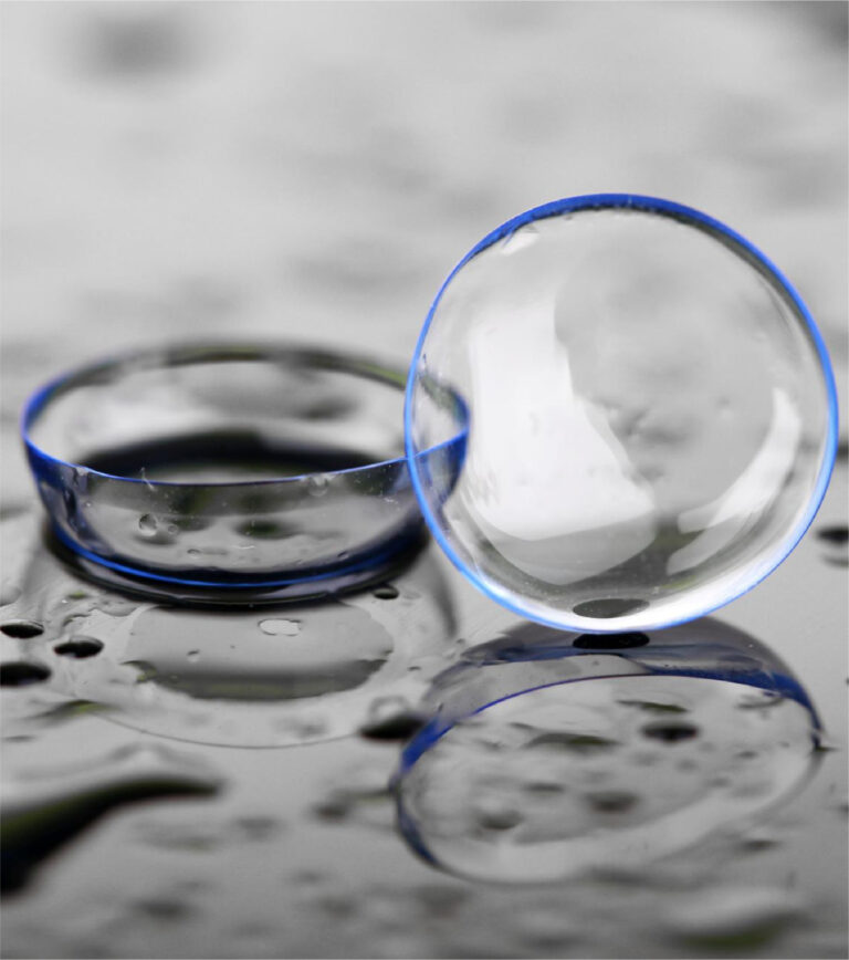
Energy & Optics
Support precision surface preparation for solar cells, optical components, lenses, and thin-film manufacturing processes in energy and optics industries.

Plasma processing prepares semiconductor and electronic components for precision assembly processes such as wire bonding, encapsulation, chip packaging, and PCB manufacturing.
Fari Plasma's semiconductor plasma equipment supports wafer-scale cleaning, ashing, and descum processes to maintain stable surface conditions for advanced semiconductor manufacturing. Plasma cleaners and plasma treatment systems remove organic residues and stabilize surface conditions without wet chemistry, reducing contamination risk and improving process consistency.

Our plasma treatment systems integrate with front-end and back-end process lines to support oxide removal and dielectric conditioning with recipe-level control. Low-damage RF and remote plasma options enable nanometer-scale cleaning and functionalization while preserving delicate device features.


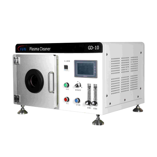
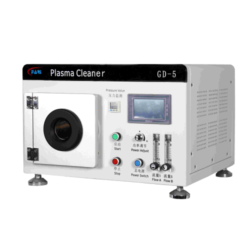
Recipe-driven RF and remote plasma control for reproducible surface treatments.

Low-energy plasma modes remove residues while preserving sensitive microstructures and device features.

Rack and inline configurations for wafer-line and roll-to-roll integration.

High-vacuum chambers with contaminant-free materials for clean processing.


Fari Plasma provides semiconductor-grade plasma cleaning and surface control, delivering low-damage, repeatable processes for electronics manufacturing.


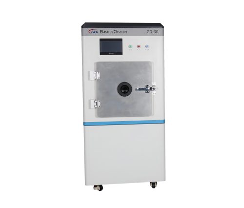
Low-energy plasma modes remove process residues while maintaining device features and critical semiconductor dimensions.

High-vacuum chambers built with contaminant-free materials ensure particle-free processing and stable conditions for semiconductor applications.

Rack, inline, and batch plasma systems integrate with front-end and back-end lines for reliable wafer and electronics production workflows.

Recipe-driven RF and remote plasma control deliver reproducible surface treatments with precise control over power, gas chemistry, and exposure time.


English

Japanese

Korean
Rogatus ad ultimum admissusque in consistorium ambage nulla praegressa inconsiderate