


Products
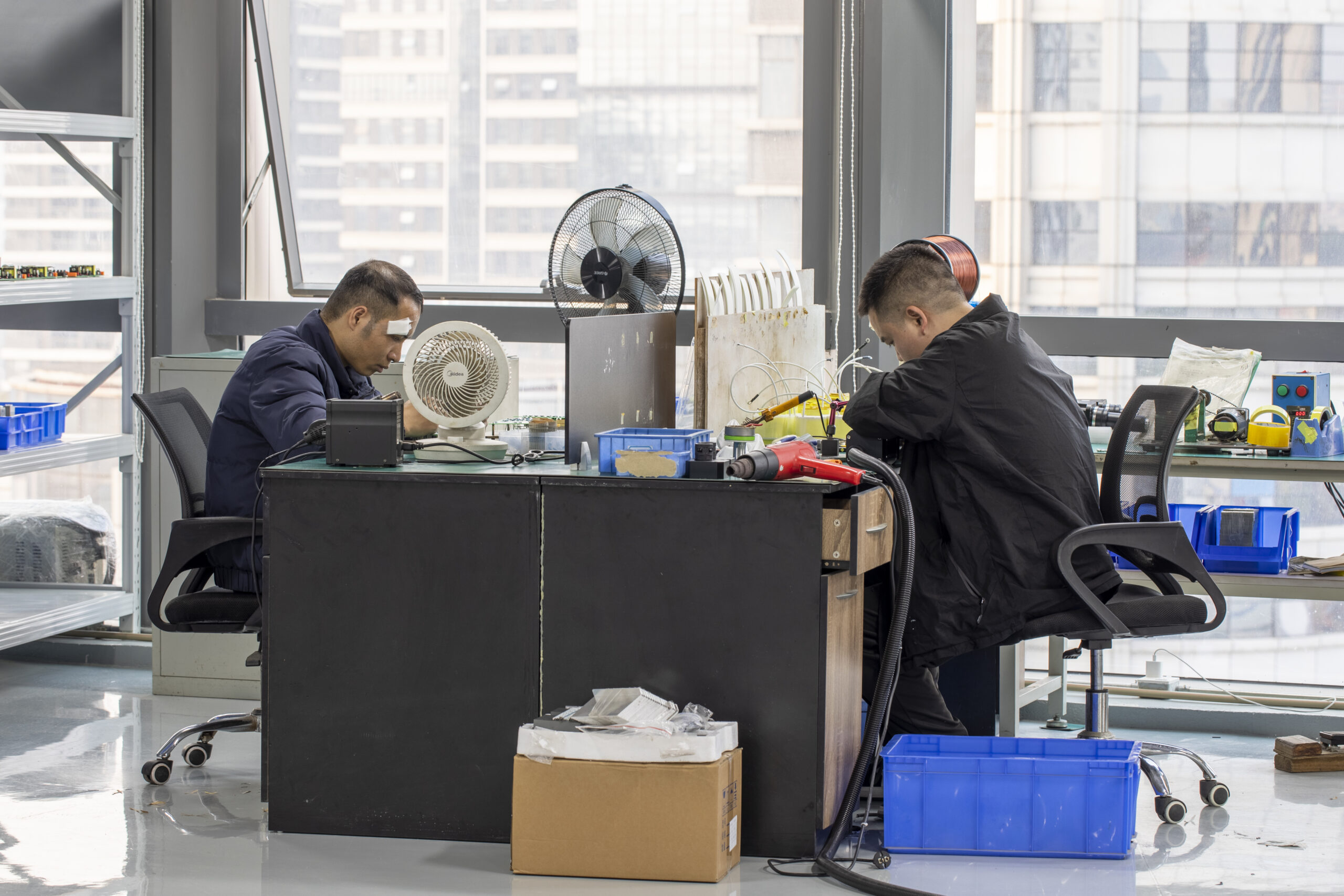
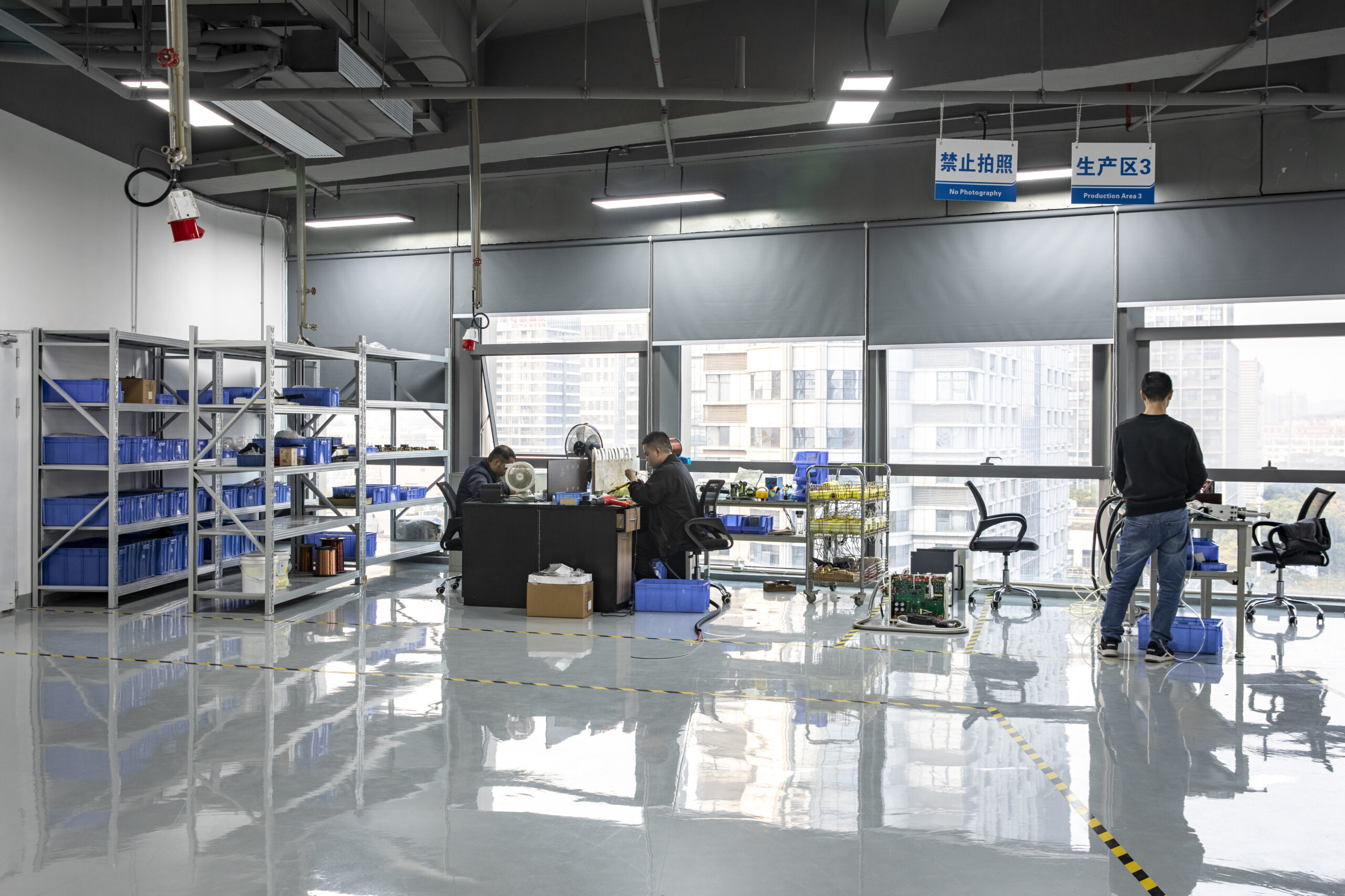
Our Semiconductor Plasma Equipment Machine
Products
-
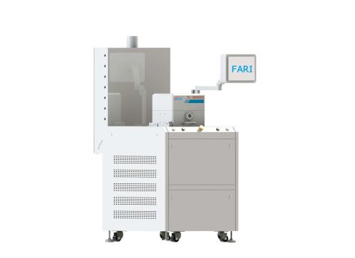
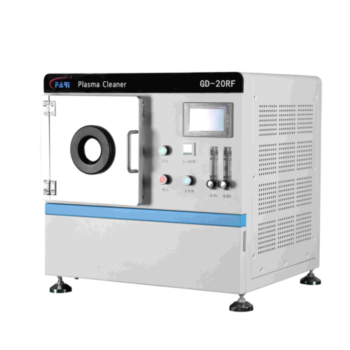 Semiconductor Plasma EquipmentGD-20RF Plasma AsherLearn More
 -
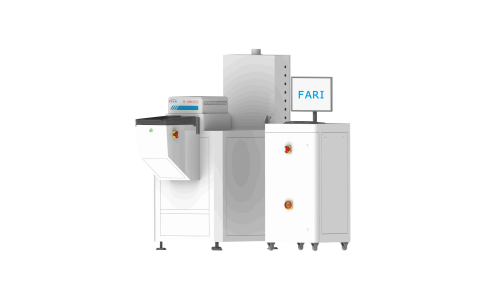
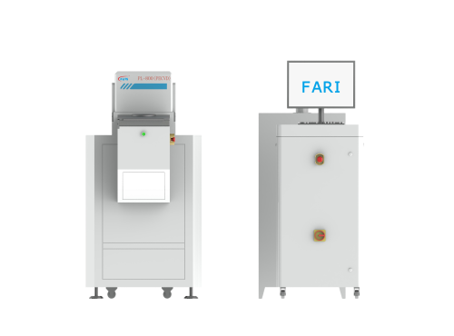
 Semiconductor Plasma EquipmentLead Frame Online Plasma CleanerLearn More
 -
 Semiconductor Plasma EquipmentSingle-Chamber RIE Reactive Ion EtcherLearn More
 -
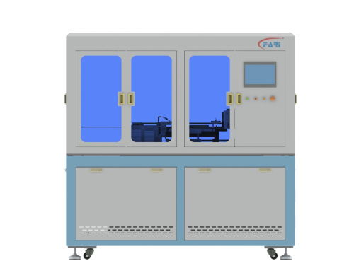
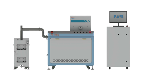
 Semiconductor Plasma EquipmentFR-G800 Dual-Chamber RIE EtcherLearn More
 -
 Semiconductor Plasma EquipmentRIE Plasma Resist Stripping SystemLearn More
 -
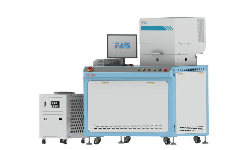
 Semiconductor Plasma EquipmentPE-200 RIE Reactive Ion EtcherLearn More
 -
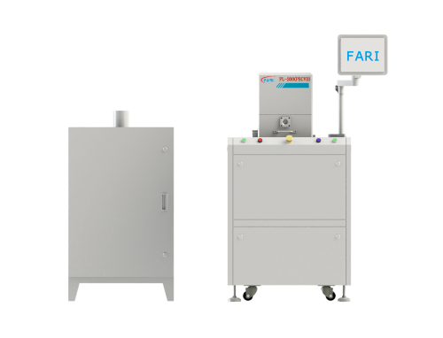
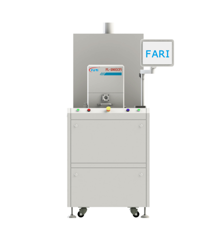
 Semiconductor Plasma EquipmentSD-300 ICP Photoresist StripperLearn More
 -
 Semiconductor Plasma EquipmentICP Plasma Residue Removal SystemLearn More
 -
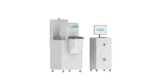
 Semiconductor Plasma EquipmentICP Inductively Coupled EtcherLearn More
 -
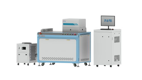
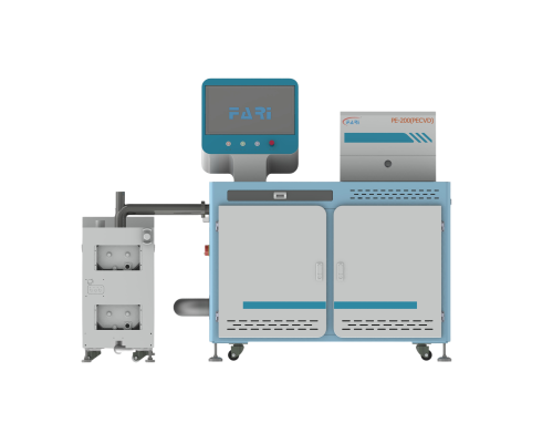
 Semiconductor Plasma EquipmentFR-G800 Dual-Chamber PECVD SystemLearn More
 -
 Semiconductor Plasma EquipmentPE-200 PECVD Thin Film SystemLearn More
 -
 Semiconductor Plasma EquipmentSingle-Chamber PECVD Deposition SystemLearn More
 -
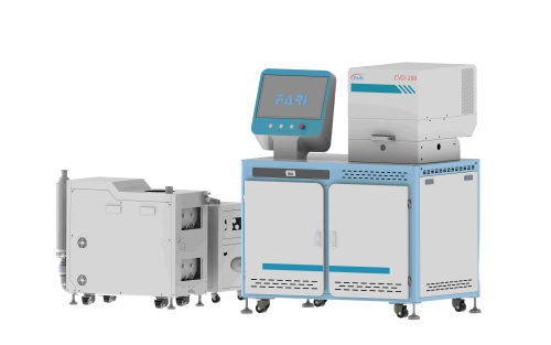
 Semiconductor Plasma EquipmentICP CVD Dual-Chamber SystemLearn More
 -
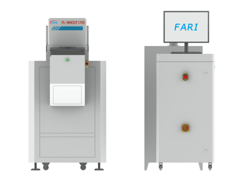
 Semiconductor Plasma EquipmentICP CVD Plasma Deposition SystemLearn More
 -
 Semiconductor Plasma EquipmentICP Inductively Coupled Plasma EtcherLearn More
 -
 Semiconductor Plasma EquipmentFR-G800 ICP Dual-Chamber EtcherLearn More