
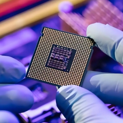
Vacuum plasma cleaning for semiconductor chips is a controlled dry process for removing trace organic contamination and preparing selected surfaces before die attach, wire or flip-chip bonding, underfill, molding or other advanced-packaging operations. It can reach small features that are difficult to wet-clean, but it must be qualified against the exact chip, package, metallization, passivation and contamination budget.
Fine-pitch packaging leaves little tolerance for residue. Flux, molding compounds, tape adhesive, handling oil, photoresist residue, particles and oxide can interfere with wetting or contact. The result may be a void, delamination, weak wire bond, unstable contact resistance or an assembly that fails after humidity and thermal cycling.
Traditional solvent, water or ultrasonic methods can leave moisture, residues, redeposition or inaccessible regions. Plasma adds a dry option, but “nano-clean” should be treated as a target to verify—not a guarantee for every feature.
Start with the fundamentals in our plasma surface-treatment overview and define whether the objective is cleaning, activation or controlled etching.
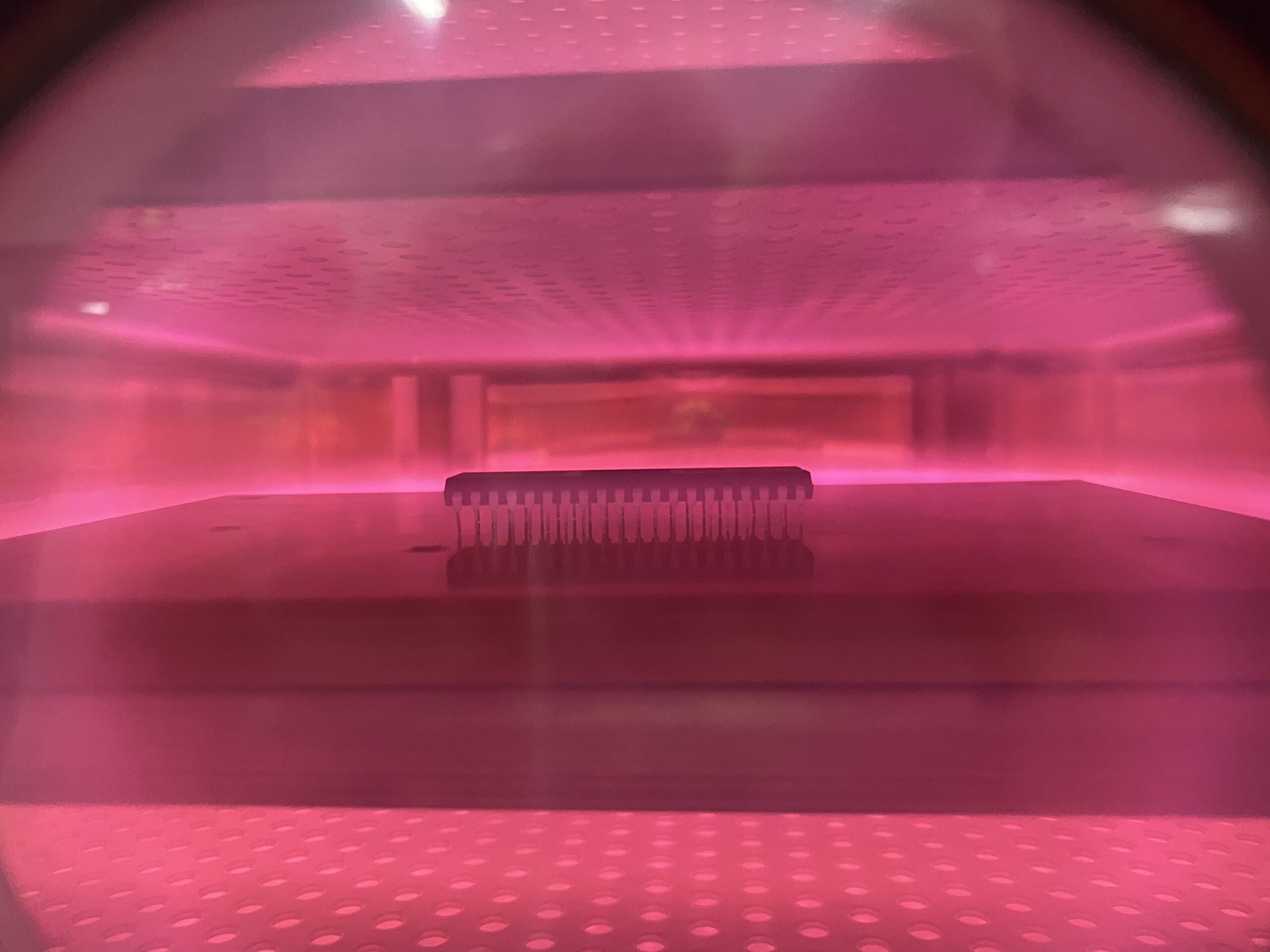
In a vacuum chamber, ions, radicals and excited species interact with exposed surfaces. Depending on the gas and dose, the process can oxidize organic residue, assist desorption, condition a thin surface layer and increase wettability for a compatible material. Chamber loading, fixture shadowing and part temperature influence uniformity.
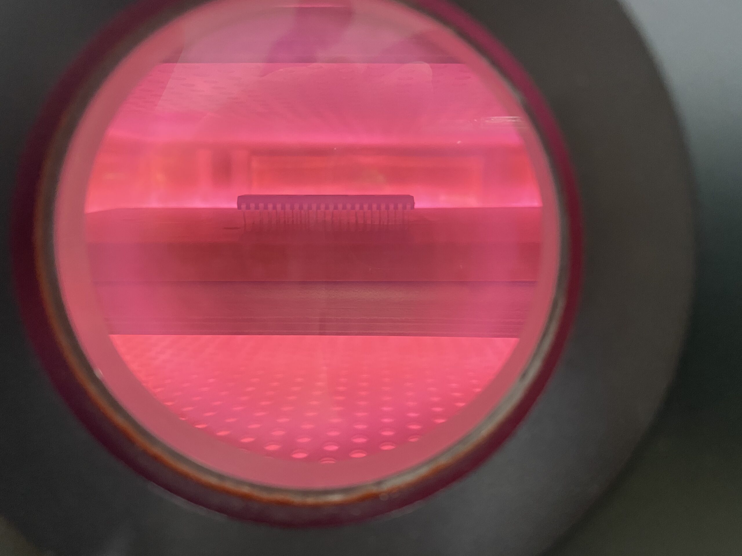
Gas selection is application-specific. Oxygen-containing processes may help with organic removal, while argon or nitrogen can provide different physical and chemical effects. Use the gas-selection guide and verify residues, electrical behavior and surface chemistry.
Plasma can prepare a die, substrate or bond pad before adhesive dispensing. Verify voiding, bond-line coverage, shear or pull strength, cure behavior and aging.
Cleaning may support more stable bonding on selected metal surfaces. It cannot replace correct wire parameters, pad metallurgy, clamping or contamination control. Measure bond pull, shear, contact resistance and failure mode.
Selected residues or organic films may be reduced before molding or rework. Protect passivation, low-k materials, solder masks and sensitive polymers from excessive dose.
Use untreated controls and a designed window for gas, power, pressure, time, temperature and loading. Surface-energy measurements can screen wetting, but pair them with XPS, FTIR, particle or ionic analysis as appropriate. The final acceptance test should be the real package function: bond strength, electrical continuity, leakage, moisture reliability and thermal cycling.
Read the limits of dyne ink, contact angle and XPS before selecting a metrology plan. Also define the time from plasma to attach or molding; activated surfaces can age and collect contamination.
For production, record recipes, chamber pressure, gas flow, endpoint indicators, maintenance, fixture condition and lot traceability. A cleanroom-compatible installation still needs validated exhaust, materials, particle controls and change management.
An incompatible dose can alter exposed metals, dielectrics, polymers or passivation. A carefully qualified process can limit risk, but electrical, mechanical and reliability checks are required on the actual device.
Vacuum treatment can improve access to small features, but coverage depends on geometry, loading and pressure. Verify the specific microstructure rather than assuming zero dead zones.
Yes. Silicon, SiC, GaN, ceramics, organic substrates and different metallizations can respond differently. Gas, dose and endpoint must be tuned to the surface stack.
There is no universal 24- or 72-hour window. Establish the maximum delay under actual packaging-room conditions and minimize handling between treatment and assembly.
It can address a verified surface-contamination or wetting contribution. Delamination may also arise from moisture, CTE mismatch, cure, package design or material selection, so root-cause analysis remains necessary.
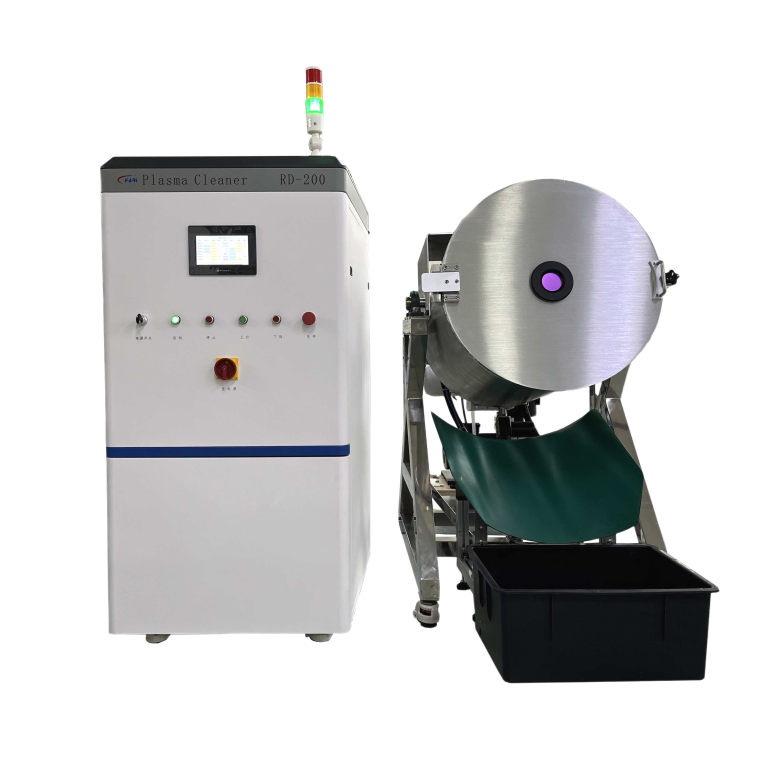
FARI Plasma can evaluate the package stack, chamber loading, contamination target and downstream reliability tests to define a controlled trial. Compare atmospheric and low-pressure formats, review available systems or contact us with sample devices and the current failure mode.



English

Spanish
Rogatus ad ultimum admissusque in consistorium ambage nulla praegressa inconsiderate