Plasma activation changes your surface chemistry to improve adhesion. Plasma cleaning removes organic contaminants without altering the base material. Plasma etching physically removes material to reshape or texturize a surface. All three use ionized gas, but they operate at different energy levels, use different process gases, and solve fundamentally different problems — choosing the wrong one can mean wasted cycle time, failed bonds, or damaged parts. This guide gives you the practical knowledge to specify the right process for your application the first time.
Think of it this way. Plasma activation is like priming a wall before painting — you’re chemically preparing the surface so something else sticks to it. Plasma cleaning is like scrubbing that wall with solvent to remove grease and dust. Plasma etching is like sanding the wall down to change its texture or remove a layer entirely.
The confusion is understandable because all three happen inside similar-looking plasma treatment systems. The hardware can even be identical. What changes is the process gas, power density, exposure time, and pressure — and those parameters determine whether you’re gently modifying the top nanometer of a polymer or aggressively carving trenches into silicon.
Here’s the critical distinction most buyers miss: activation and cleaning are surface-preparation steps that preserve your part geometry. Etching is a material-removal step that intentionally changes it. If you conflate them, you’ll either under-treat (leading to adhesion failures) or over-treat (damaging sensitive components).
Plasma activation grafts polar functional groups — hydroxyl (–OH), carboxyl (–COOH), amino (–NH₂) — onto an otherwise inert surface. Polymers like polypropylene, PEEK, and PTFE are notoriously difficult to bond or print on because their surface energy is too low. Water beads up. Adhesives peel off. Inks smear. Activation fixes this by breaking C–H and C–C bonds on the top 1–10 nanometers and replacing them with oxygen- or nitrogen-containing groups that dramatically raise surface energy.
A typical polypropylene surface sits around 29–31 mN/m surface energy. After 5–15 seconds of oxygen plasma activation, that jumps to 55–72 mN/m — well above the threshold needed for reliable adhesive bonding or coating adhesion. No material is removed. The part dimensions don’t change. You’re just rewriting the chemistry of the outermost molecular layer.
A European automotive tier-1 supplier was experiencing a 12% rejection rate on dashboard trim pieces where a decorative film delaminated from a PP substrate after thermal cycling. Solvent-based primers added cost and VOC concerns. After integrating inline atmospheric plasma activation at the lamination station, surface energy rose from 30 mN/m to 62 mN/m, delamination failures dropped below 0.3%, and the primer step was eliminated entirely — saving roughly €0.40 per part.
Activated surfaces don’t stay activated forever. Those polar groups rearrange and migrate back into the bulk polymer over hours to days, depending on the material and storage conditions. For most polymers, you want to bond or coat within minutes to a few hours of treatment. This is why inline integration matters — and why batch activation with long storage before the next process step is risky. Check our technology and knowledge hub for more on aging behavior and how to manage it.
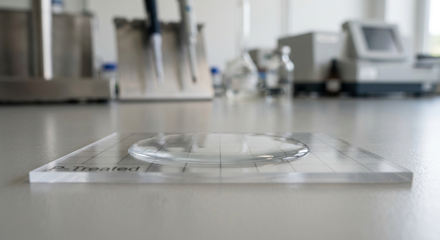
Plasma cleaning uses reactive species — primarily oxygen radicals and UV photons from an O₂ or air plasma — to volatilize organic contaminants. Fingerprint oils, mold-release agents, machining residues, and hydrocarbon films are broken down into CO₂, H₂O, and other volatile byproducts that get pumped away. Argon plasma can also be used for a more physical sputtering-type clean, knocking off loosely bound particles through ion bombardment.
The key difference from activation: cleaning targets contaminants that are on the surface, not the surface material itself. You’re removing something that shouldn’t be there. Material removal from the substrate is typically in the single-digit nanometer range — negligible for any practical geometry concern.
Plasma cleaning is particularly powerful where wet cleaning fails or introduces new problems. Solvent cleaning can leave residue films. Ultrasonic baths may not reach micro-features. Plasma reaches everywhere the gas can flow — including blind holes, complex geometries, and porous surfaces.
A medical device manufacturer producing titanium bone screws found that residual machining coolant caused inconsistent hydroxyapatite coating adhesion, leading to batch failures during quality testing. Switching from multi-stage aqueous cleaning to a 3-minute low-pressure O₂ plasma clean reduced organic contamination to below XPS detection limits and improved coating pull-off strength by 40%. The process also eliminated wastewater disposal costs from the old cleaning line.
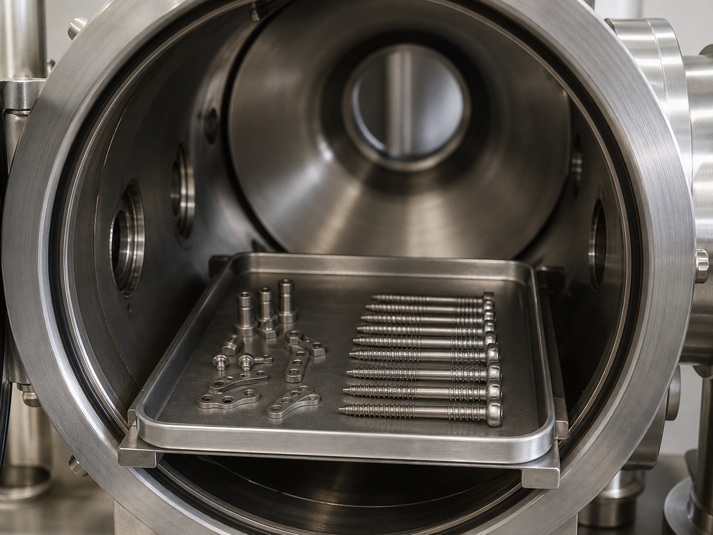
Plasma etching is where things get aggressive — intentionally. Unlike activation and cleaning, etching removes meaningful amounts of substrate material. Etch rates can range from tens of nanometers per minute to several micrometers per minute, depending on the gas chemistry, power, and substrate.
There are two main flavors:
Most real-world etching processes use a combination of both — reactive ion etching (RIE) — to balance selectivity, etch rate, and profile control.
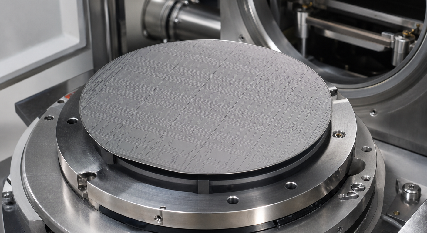
One of etching’s superpowers is selectivity. With the right gas chemistry, you can etch silicon dioxide 20–50× faster than the underlying silicon. Or strip a polymer layer off a metal substrate without touching the metal. This is what makes plasma etching indispensable in semiconductor manufacturing — it’s not just about removing material, it’s about removing the right material at the right rate with nanometer-level precision.
Here’s the comparison that should clarify your decision. If you take away one thing from this article, let it be this table:
| Criteria | Plasma Activation | Plasma Cleaning | Plasma Etching |
|---|---|---|---|
| Primary Purpose | Add functional groups to surface | Remove organic contaminants | Remove bulk material / texturize |
| Material Removal | Negligible | Minimal (nanometer scale) | Significant (µm scale possible) |
| Typical Process Gas | O₂, N₂, NH₃ | Ar, O₂, air | CF₄, SF₆, O₂, Ar |
| Treatment Depth | Top 1–10 nm | Top 1–50 nm | Hundreds of nm to µm |
| Effect Duration | Hours to days (aging) | Permanent (contaminant removed) | Permanent (material removed) |
| Common Industries | Automotive, packaging, textiles | Medical devices, electronics, optics | Semiconductors, MEMS, PCB |
| Process Complexity | Low to moderate | Low | Moderate to high |
| Risk of Surface Damage | Very low | Low | Moderate (intentional removal) |
Notice the pattern: as you move from activation to cleaning to etching, energy input increases, material removal increases, and process complexity increases. Most industrial applications actually need activation or cleaning — etching is primarily a semiconductor and microfabrication tool.
Here’s something that trips up first-time buyers: these processes aren’t always mutually exclusive. In fact, a single plasma treatment cycle often performs cleaning and activation simultaneously.
When you run an oxygen plasma on a polymer part, the first few seconds clean off surface hydrocarbons. The next several seconds begin activating the now-clean surface. You get both effects in one step. This is one reason plasma treatment is so efficient compared to multi-stage wet chemical processes — you’re collapsing two preparation steps into one.
Some applications require a deliberate two-step approach:
The point is: don’t think of these as three separate machines or three separate purchase decisions. Often it’s one system with different recipes. The right plasma system capabilities let you switch between modes by changing the gas, power, and time parameters.
Still unsure which process you need? Walk through these three questions:
If your bonding or coating failure is caused by contamination — oils, fingerprints, release agents — you need cleaning. If the surface is already clean but the material itself has low surface energy (most polymers, silicones, fluoropolymers), you need activation. Simple contact angle measurements can tell you which situation you’re in. A clean but inert surface will show a high contact angle with uniform droplet shape. A contaminated surface will show inconsistent contact angles across different spots.
If yes — whether it’s stripping a coating, creating micro-textures, or patterning features — you need etching. If you just need to prepare the existing surface for the next process step without changing its geometry, etching is overkill and risks damaging your part.
The downstream process determines your requirements:
When in doubt, reach out to our applications team with your substrate material, current failure mode, and downstream process. We can typically recommend the right approach within a day.
After working with hundreds of manufacturers, certain mistakes come up again and again:
We see this especially with engineers coming from semiconductor backgrounds who default to “etch” as a catch-all term. If you’re bonding PEEK to aluminum in an aerospace assembly, you don’t want to etch the PEEK — you want to activate it. Etching would roughen the surface and potentially compromise the part’s mechanical properties.
Activating parts on Monday and bonding them on Thursday is a recipe for inconsistent results. Activated surfaces lose 30–60% of their gained surface energy within 24–72 hours on most polymers. Design your line so that activation happens immediately before the bonding or coating step.
Compressed air plasma is cheap and convenient — and it’s perfectly adequate for many cleaning and activation jobs. But if you need nitrogen-containing functional groups for specific adhesive chemistries, or if you need fluorine-based etching, air won’t cut it. Specify the gas chemistry based on the surface chemistry you need, not based on what’s easiest to supply.
More plasma is not always better. Thin polymer films, delicate electronic components, and biological substrates can be damaged by excessive power or treatment time. Always run a dose-response study — treat samples at increasing power/time combinations and measure the result — before locking in production parameters.
Yes, significantly. The choice between atmospheric-pressure and low-pressure (vacuum) plasma affects which of the three processes you can run effectively.
Operates at ambient pressure using a plasma jet or corona-style discharge. Excellent for inline activation and cleaning of flat or moderately contoured surfaces. Fast, easy to integrate into existing production lines, and requires no vacuum chamber. However, atmospheric plasma is generally limited to activation and light cleaning. You won’t achieve precise etching with atmospheric systems — the plasma is less uniform and the reactive species have shorter mean free paths.
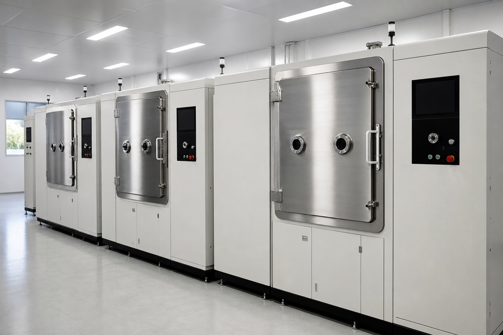
Operates in a vacuum chamber at pressures typically between 0.1 and 1 mbar. Provides highly uniform treatment across complex 3D geometries and batch loads. Essential for etching applications where you need controlled, repeatable material removal. Also preferred for cleaning and activation of medical devices and electronics where uniformity and process documentation are critical.
The short version: if you need etching, you almost certainly need low-pressure. If you need inline activation of parts moving on a conveyor, atmospheric is usually the better fit. Cleaning can go either way depending on part geometry and cleanliness requirements. Explore both options in our plasma treatment services overview.
The difference between plasma activation, cleaning, and etching isn’t academic — it directly affects your process yield, part quality, and equipment investment. Activation modifies chemistry. Cleaning removes contamination. Etching removes material. Get the distinction right, and you’ll specify a system that solves your actual problem on the first try.
If you’re evaluating plasma treatment for a specific application, the fastest path forward is a process trial. Send us your parts, tell us what’s failing or what you’re trying to achieve, and our applications engineers will run test treatments and deliver measured results — contact angle data, surface energy values, or etch depth profiles depending on what you need. Visit our contact page to start that conversation.



English

Spanish
Rogatus ad ultimum admissusque in consistorium ambage nulla praegressa inconsiderate