
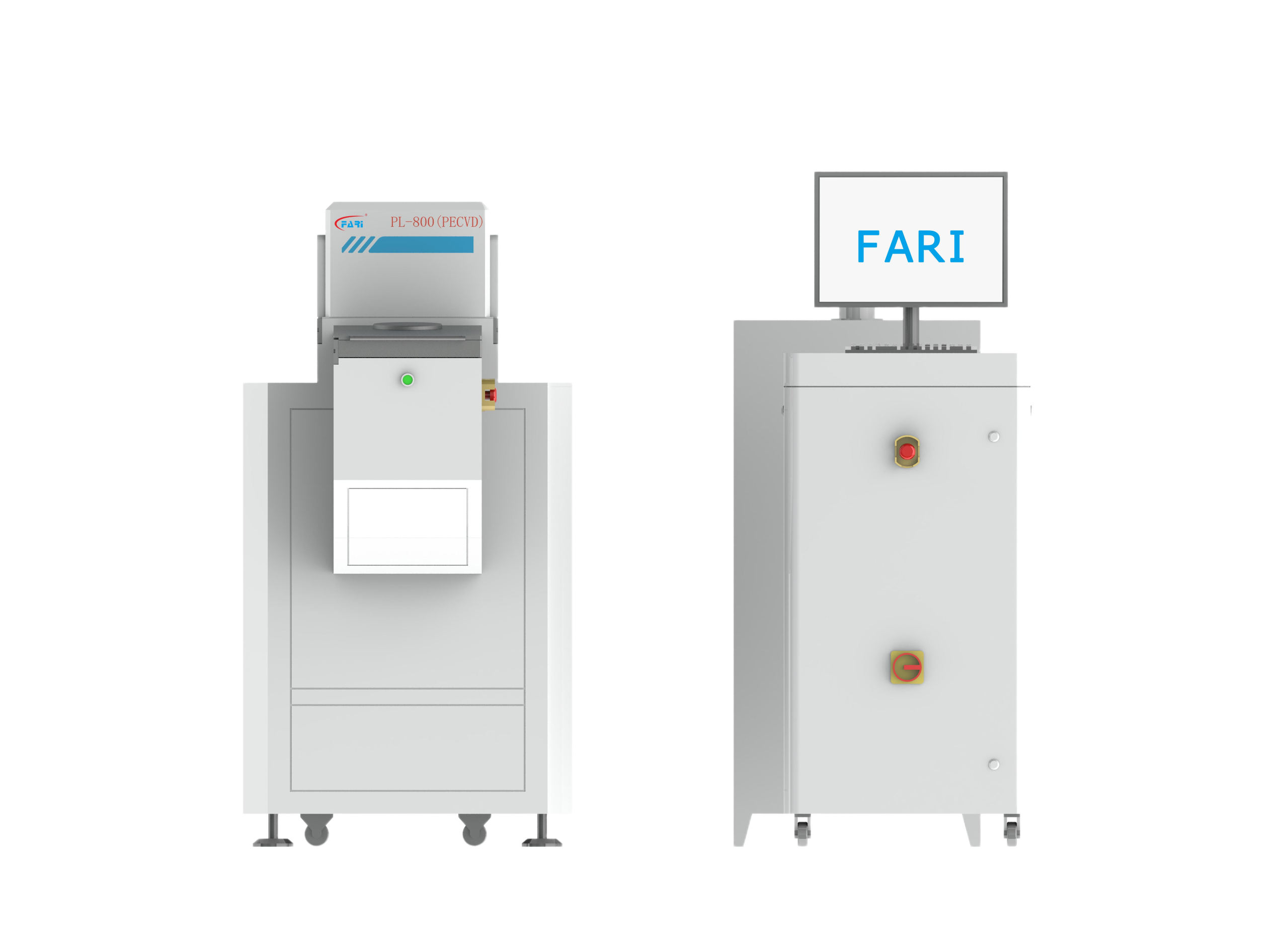
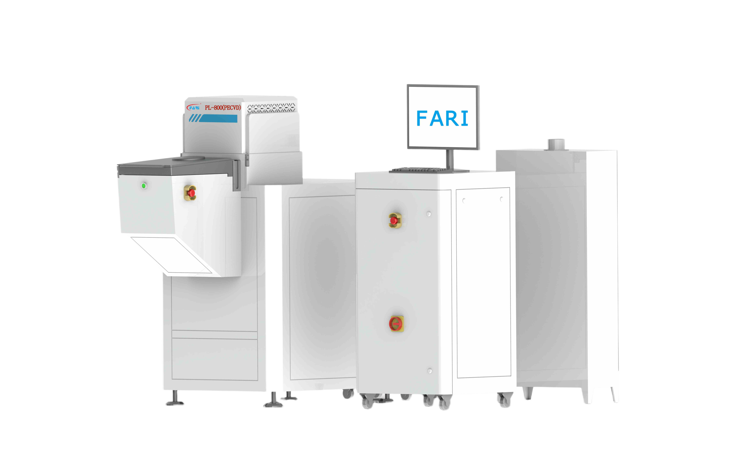
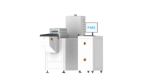
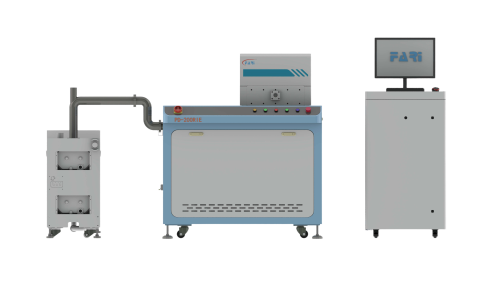
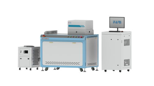
FR-G800 PECVD is a dual-chamber plasma-enhanced CVD system for low-temperature deposition of high-quality dielectric and optical thin films. It supports 2–8" wafers and broad R&D and production needs.
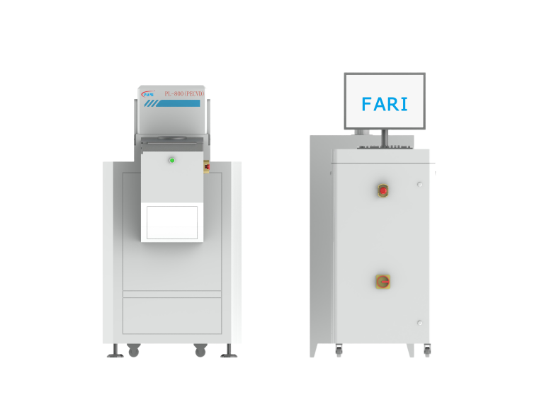
| Process Type | PECVD (Plasma Enhanced Chemical Vapor Deposition) |
| Model | FR-G800 |
| Chamber Configuration | Dual-chamber |
| Temperature Range | 100–400 °C |
| Wafer Sizes Supported | 2, 3, 4, 6, 8 inch |
| Discharge Methods | DC / AC / RF / Microwave / ECR |
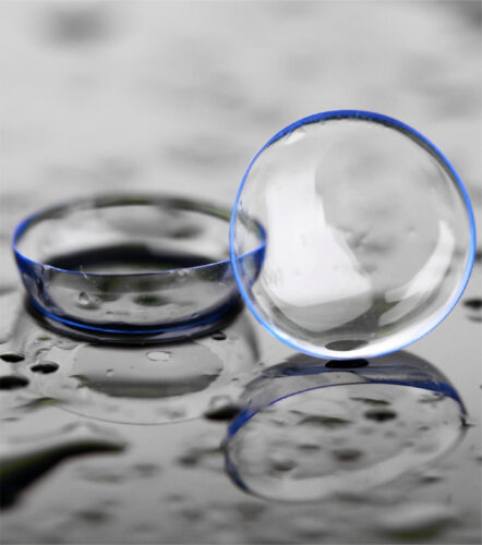
| Typical Deposited Materials | Dielectric and optical thin films (e.g., SiOx, SiNx, low-k materials) |
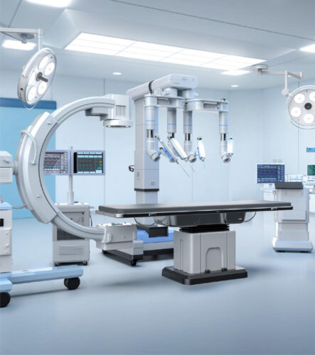
| Primary Applications | Semiconductors, photonics, photovoltaics, biomedical devices |


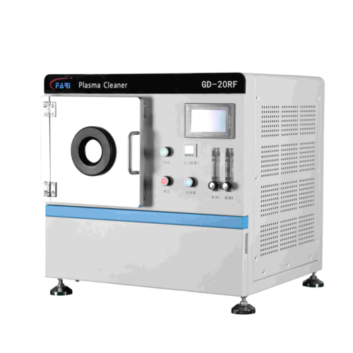
Process gas is energized and converted into a reactive plasma containing ions, electrons, and radicals.

High-energy plasma species reach the material surface and interact with contaminants at the molecular level.

Reactive ions and radicals break down organic residues and surface contaminants through controlled chemical reactions.

The reaction products are converted into volatile compounds and enter the gas phase.

Gaseous by-products desorb from the surface and are evacuated, leaving a clean, activated material surface.

English

Japanese

Korean
Rogatus ad ultimum admissusque in consistorium ambage nulla praegressa inconsiderate