Semiconductor Plasma Equipment

ICP CVD Dual-Chamber System

High-density ICP CVD dual-chamber system for deposition of SiN, SiO2 and a-Si films. Delivers uniform, reproducible thin films and advanced composite deposits for semiconductor, solar and related industries.
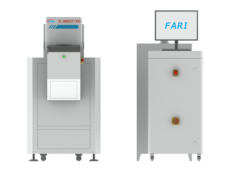
  • High-density ICP for uniform films.
  • Dual-chamber design for increased throughput.
  • Versatile deposition for SiN, SiO2, a-Si.

Tech Specs

System Type Inductively Coupled Plasma Chemical Vapor Deposition (ICP-CVD)
Configuration Dual-chamber design for parallel processing and higher throughput
Target Films Silicon nitride (SiN), silicon dioxide (SiO2), amorphous silicon (a-Si) and composite deposits
Main Components Reaction chambers, vacuum system, gas delivery system, RF power supply, and integrated control system
Plasma Source Inductive RF excitation producing high-density plasma and abundant reactive species
Primary Functions Thin film deposition, surface modification, and composite material growth via plasma-driven chemistry

Key Features

  • High-Density Plasma Generation

    Inductively coupled RF source creates a high-density plasma that produces abundant reactive species, enabling fast, conformal deposition and excellent film quality across substrates.

  • Dual-Chamber Throughput Design

    Dual-chamber architecture supports parallel processing or staged workflows to increase productivity while minimizing cross-contamination and downtime between runs.

  • Broad Material Compatibility

    Engineered for SiN, SiO2, a-Si and specialty composite deposits, the system handles diverse precursor chemistries for semiconductor, photovoltaic and coating applications.

  • Integrated Vacuum And Gas Controls

    Precision vacuum and gas delivery subsystems maintain stable process conditions and repeatability, ensuring uniform film thickness, stoichiometry and reduced defectivity.

  • Stable RF Power And Process Control

    Robust RF power supply and closed-loop control enable consistent plasma conditions and repeatable deposition recipes for high-yield production and R&D tasks.

  • Application-Focused Flexibility

    Modular design supports recipe customization and process tuning for applications ranging from semiconductor passivation to solar cell and composite material enhancement.

Plasma Cleaning Process

  • Plasma Generation

    Process gas is energized and converted into a reactive plasma containing ions, electrons, and radicals.

  • Plasma–Surface Interaction

    High-energy plasma species reach the material surface and interact with contaminants at the molecular level.

  • Chemical Reaction

    Reactive ions and radicals break down organic residues and surface contaminants through controlled chemical reactions.

  • Volatilization

    The reaction products are converted into volatile compounds and enter the gas phase.

  • Removal from Surface

    Gaseous by-products desorb from the surface and are evacuated, leaving a clean, activated material surface.