
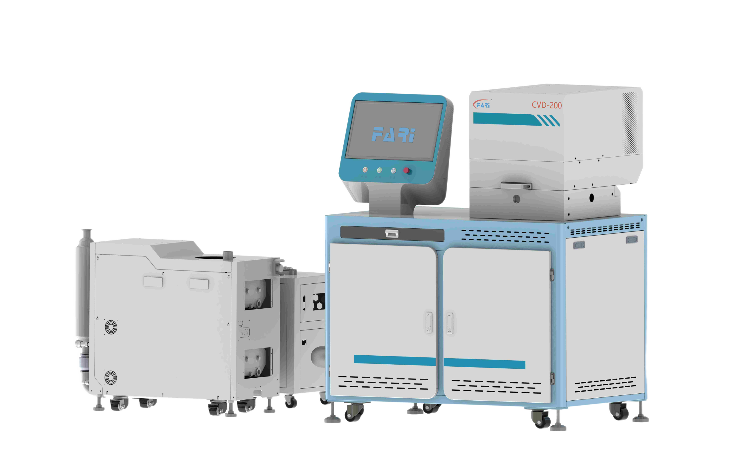
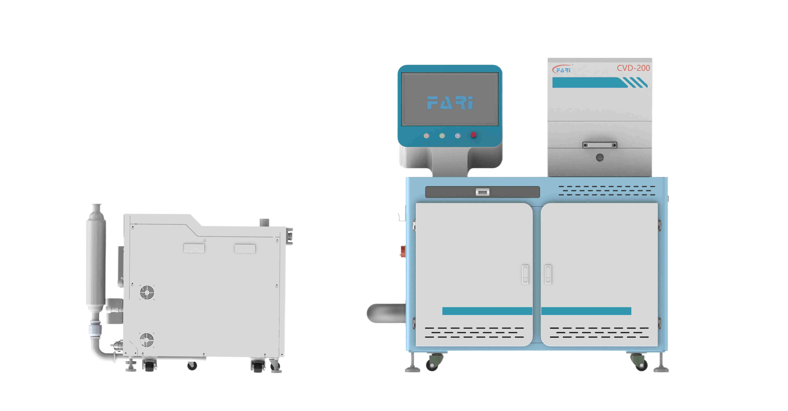
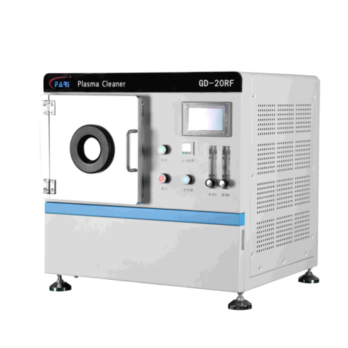
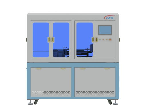
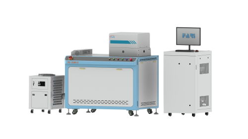
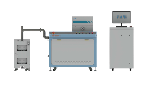
A high-density ICP CVD plasma deposition system engineered for uniform, low-contamination thin film growth on wafers and substrates. Ideal for semiconductor, MEMS, and specialty coating applications requiring precise process control.

| Wafer Size | Up to 200 mm (8 inch) substrates |
| Chamber Volume | Compact vacuum chamber suitable for single-wafer processing |
| ICP Power | 0–2000 W (adjustable) |
| RF Bias Power | 0–500 W (process bias control) |
| Process Pressure | 0.1–100 Pa (≈0.75–750 mTorr) |
| Base Vacuum | < 5 × 10^-6 Torr |
| Temperature Range | Ambient to 400 °C (substrate heater) |
| Deposition Rate | Typical 5–200 nm/min (process dependent) |
| Uniformity | ±3% across usable wafer area |
| Process Gases | SiH4, NH3, N2, O2, Ar and other specialty precursors |
| Control Interface | PLC with touchscreen and recipe management |


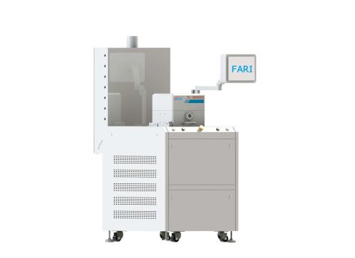
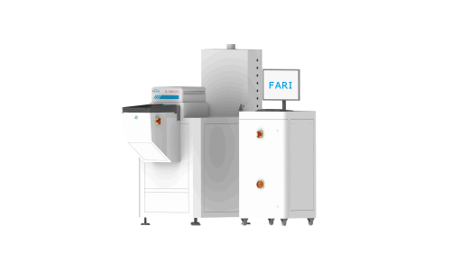
Process gas is energized and converted into a reactive plasma containing ions, electrons, and radicals.

High-energy plasma species reach the material surface and interact with contaminants at the molecular level.

Reactive ions and radicals break down organic residues and surface contaminants through controlled chemical reactions.

The reaction products are converted into volatile compounds and enter the gas phase.

Gaseous by-products desorb from the surface and are evacuated, leaving a clean, activated material surface.

English

Japanese

Korean
Rogatus ad ultimum admissusque in consistorium ambage nulla praegressa inconsiderate