

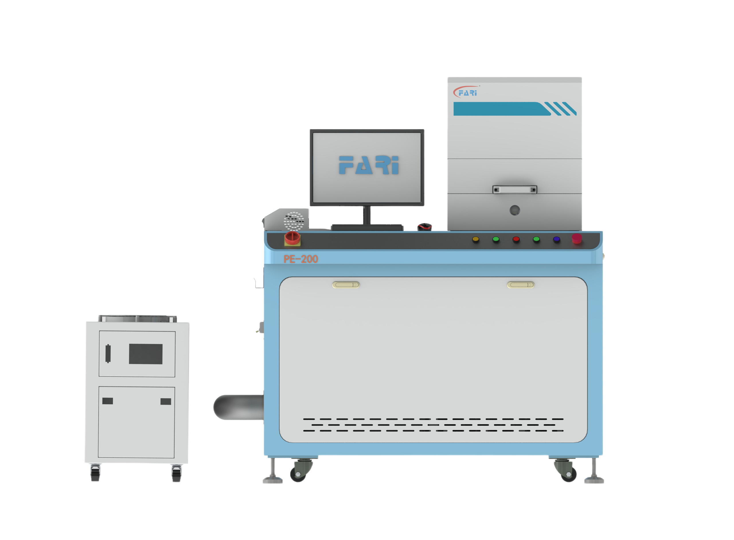
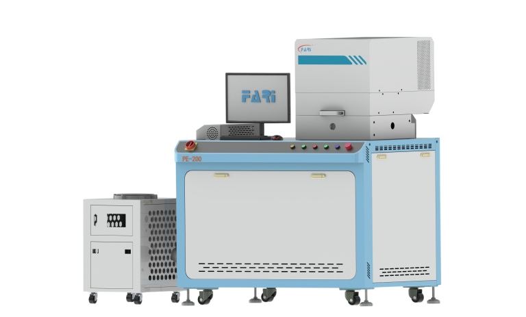
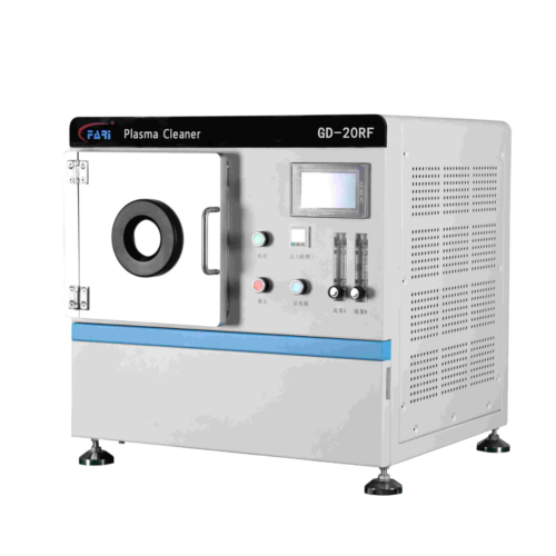
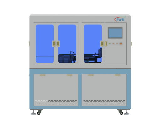
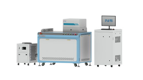
High-density ICP etcher using dual RF sources for rapid, uniform etching of dielectrics, metals and compound semiconductors. Dual-chamber design minimizes contamination and ensures operator safety.
| Plasma Type | Inductively Coupled Plasma (ICP) |
| RF Sources | Inductive RF generator for plasma + RF substrate bias generator |
| Chamber Configuration | Pre-vacuum chamber and reaction chamber for contamination control |
| Main Components | Reaction chamber, upper and lower electrodes, RF sources, vacuum system, gas control, cooling system, backside helium control, control software |
| Process Gases | Configurable gas delivery for fluorine-, chlorine-, oxygen-based chemistries |
| Cooling System | Closed-loop refrigeration for wafer and system temperature stability |
| Backside Helium Control | Integrated He backfill and control for thermal conduction and chucking |
| Control & Software | Recipe management, process monitoring, operator interface and automation support |
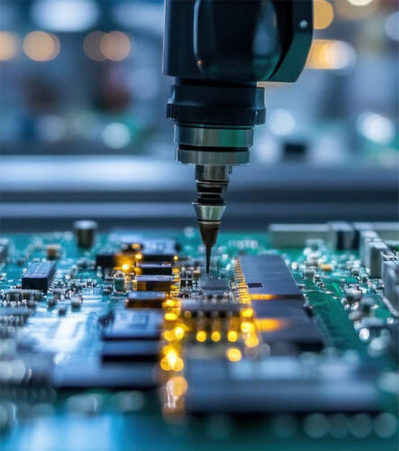
| Target Materials | Oxides, nitrides, metals and III-V compound semiconductors (e.g., SiO₂, Si₃N₄, Al, GaAs) |


Process gas is energized and converted into a reactive plasma containing ions, electrons, and radicals.

High-energy plasma species reach the material surface and interact with contaminants at the molecular level.

Reactive ions and radicals break down organic residues and surface contaminants through controlled chemical reactions.

The reaction products are converted into volatile compounds and enter the gas phase.

Gaseous by-products desorb from the surface and are evacuated, leaving a clean, activated material surface.

English

Japanese

Korean
Rogatus ad ultimum admissusque in consistorium ambage nulla praegressa inconsiderate