
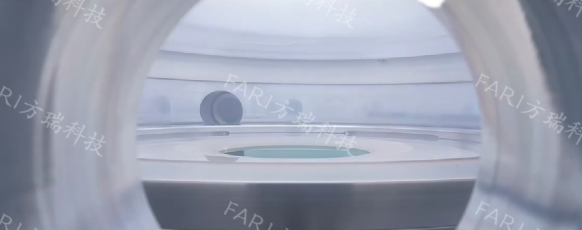
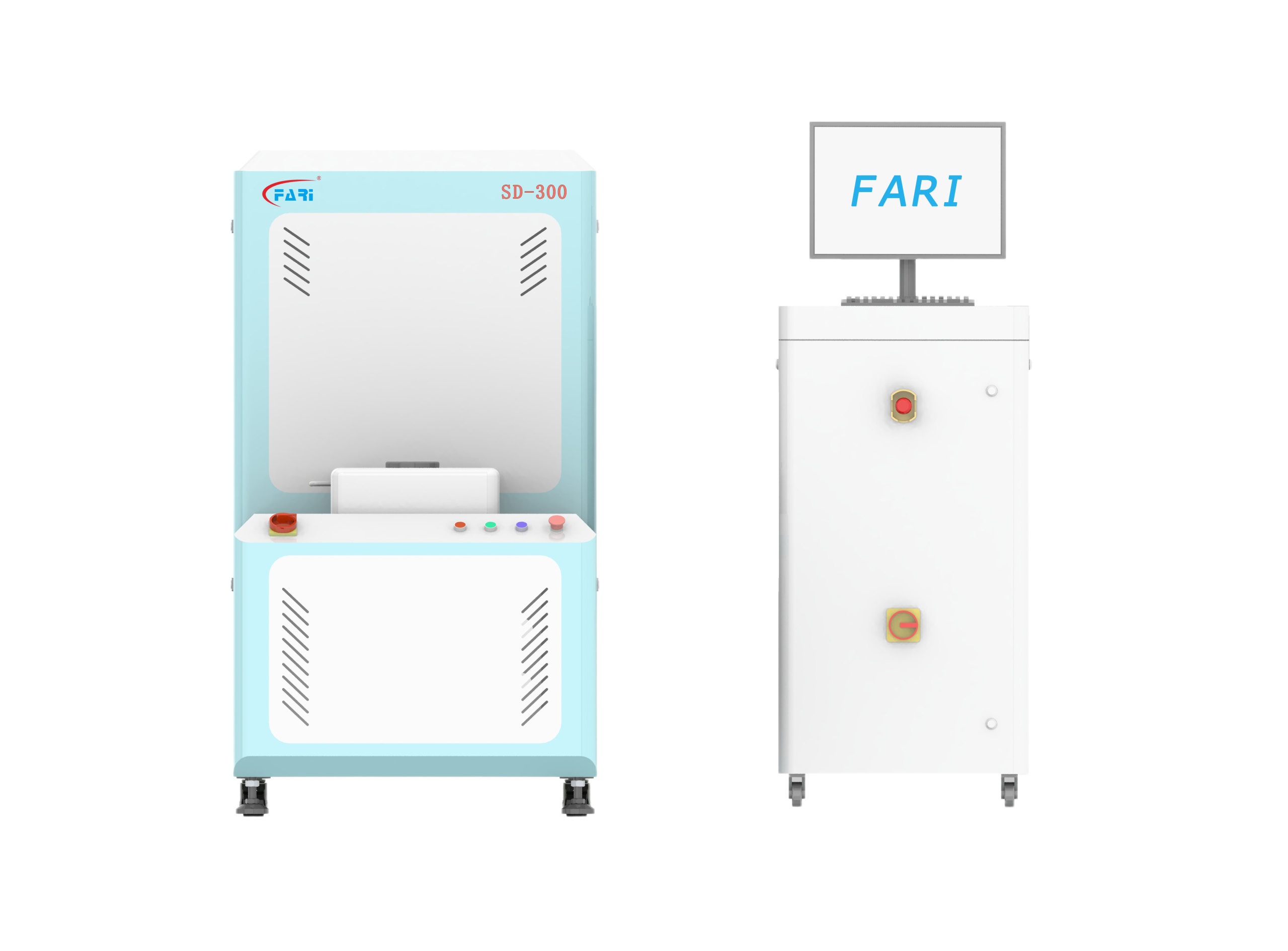
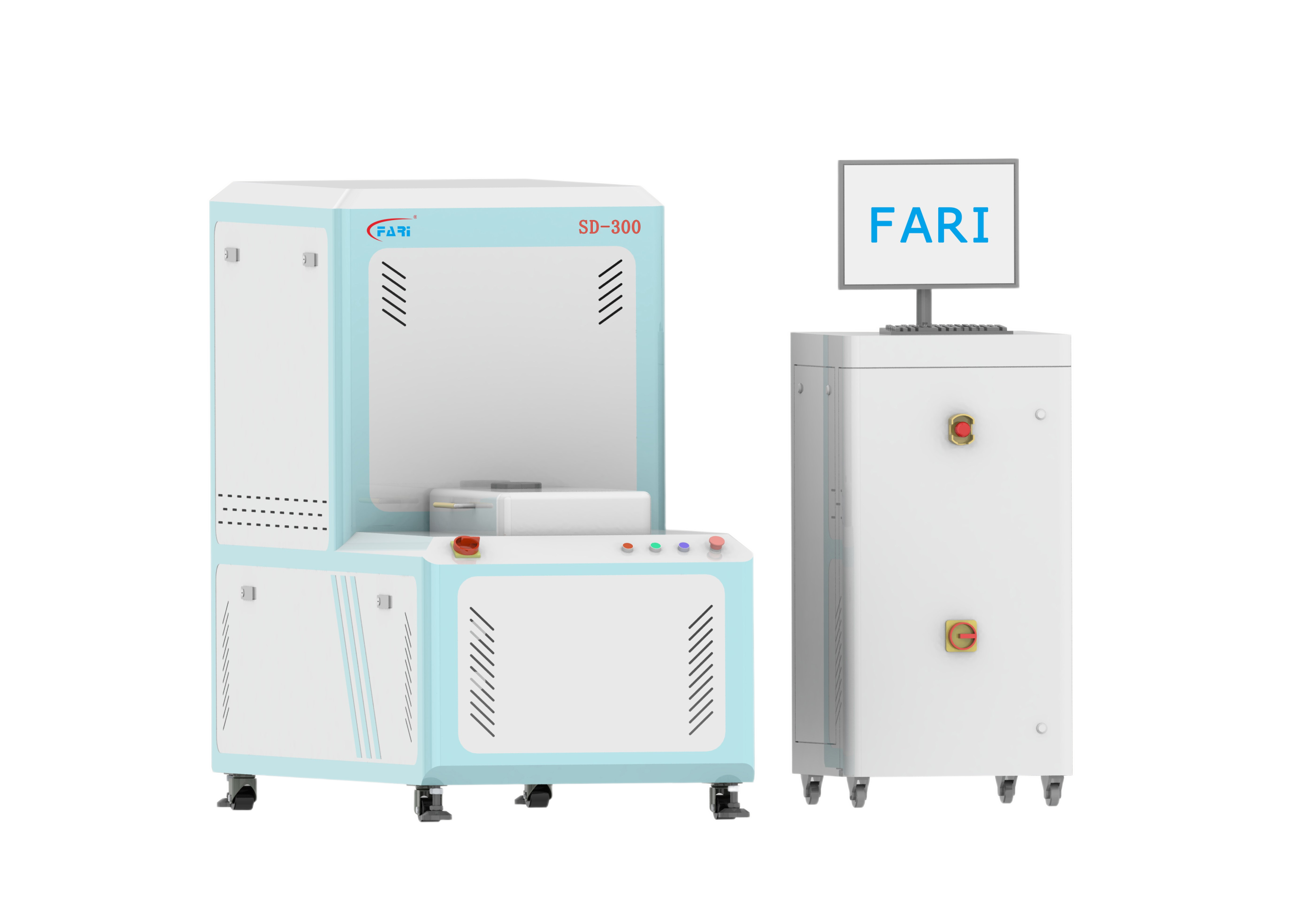

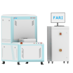
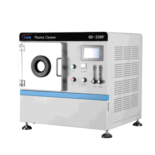
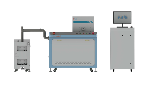
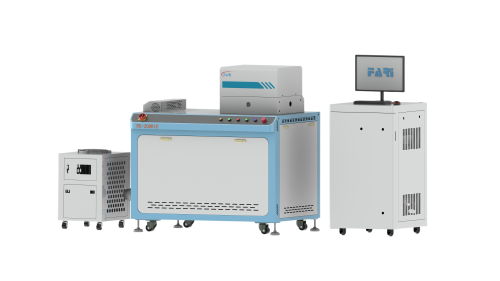
The SD-300 is an ICP-based photoresist stripper designed for high-efficiency removal of photoresist, organic residues and nanoscale contaminants in advanced semiconductor, packaging and display processes. It offers eco-friendly operation, flexible process control and high uniformity for reliable production.
| Model | SD-300 |
| PlasmaSource | RF 13.56 MHz |
| RFPower | 2 kW |
| WaferCompatibility | 2, 4, 6, 8 inch |
| BatchProcessing | Multi-wafer (multi-wafer processing only for 2" and 4" wafers) |
| Dimensions | 673 × 1455 × 1695 mm (L × W × H) |
| ChamberConfiguration | Load lock + process chamber |
| ProcessTemperatureRange | 50–250 °C |
| Uniformity | ≤5% (edge exclusion 10 mm, 5-point measurement, Max-Min/(2*mean)) |
| LowTemperatureResistRemoval | Process temperature ≤90 °C, removal rate 50–100 nm/min, uniformity ≤5%, 5-area thickness test |
| HighTemperatureAshing | Process temperature ≤250 °C, removal rate 3000–5000 nm/min, uniformity ≤5%, 5-area thickness test |
| ControlSystem | FR system (FangRui) |
| AutomationLevel | Manual to semi-automatic |
| Chiller | Electrode cooling FR-600A-H |


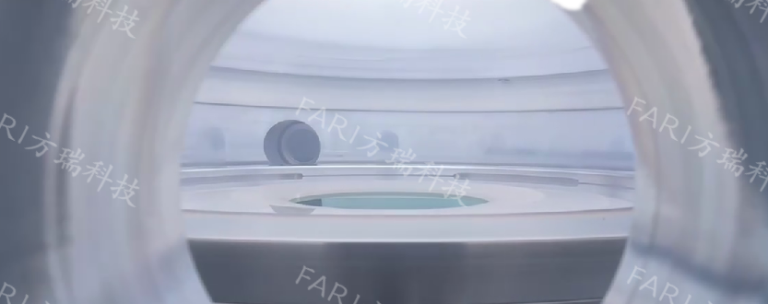
Process gas is energized and converted into a reactive plasma containing ions, electrons, and radicals.

High-energy plasma species reach the material surface and interact with contaminants at the molecular level.

Reactive ions and radicals break down organic residues and surface contaminants through controlled chemical reactions.

The reaction products are converted into volatile compounds and enter the gas phase.

Gaseous by-products desorb from the surface and are evacuated, leaving a clean, activated material surface.

English

Japanese

Korean
Rogatus ad ultimum admissusque in consistorium ambage nulla praegressa inconsiderate