Semiconductor Plasma Equipment

Single-Chamber PECVD Deposition System

Single-chamber PECVD system for low-temperature plasma-enhanced deposition of SiO2 and dielectric thin films. Optimized for high-quality, dense layers used in semiconductors, photovoltaics, and photonics.
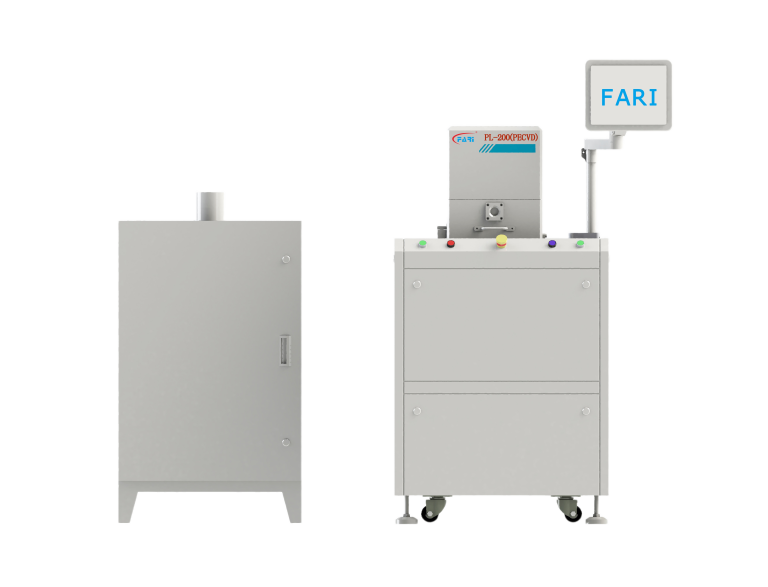
  • Low-temperature deposition for temperature-sensitive substrates
  • High-quality SiO2 and dielectric film deposition
  • Single-chamber design with RF/Microwave/ECR plasma options

Tech Specs

Process Plasma Enhanced Chemical Vapor Deposition (PECVD)
Film Type SiO2 and other dielectric thin films
Temperature Range 200-400 °C
Chamber Configuration Single chamber
Plasma Sources DC/AC, RF, Microwave, Electron Cyclotron Resonance (ECR)
Primary Applications Semiconductors, photovoltaics, optoelectronics, biomedical

Key Features

  • Low-Temperature Deposition for Sensitive Substrates

    Enables deposition at reduced temperatures (typically 200–400 °C), minimizing thermal stress on substrates and allowing processing of temperature-sensitive materials while maintaining film quality.

  • High Film Quality and Uniformity Control

    Delivers dense, uniform dielectric and SiO2 films with controlled stoichiometry and low defects, improving device performance and reliability across large substrates and wafers.

  • Versatile Gas Chemistry and Process Flexibility

    Supports a wide range of precursor gases and process recipes to tailor film composition, refractive index, and electrical properties for diverse applications from optics to microelectronics.

  • Single-Chamber Modular System Design

    Compact single-chamber architecture simplifies integration, reduces footprint and contamination risk, and enables efficient throughput for R&D and pilot production environments.

  • Precise Thickness and Deposition Rate Control

    Offers accurate control of deposition rate and film thickness through optimized RF/microwave power and gas flow management, ensuring repeatable thin-film stacks and critical layer tolerances.

  • Improved Adhesion and Film Density

    Plasma activation and energetic species promote strong film adhesion and high density, enhancing mechanical stability and long-term performance of coated devices and components.

Plasma Cleaning Process

  • Plasma Generation

    Process gas is energized and converted into a reactive plasma containing ions, electrons, and radicals.

  • Plasma–Surface Interaction

    High-energy plasma species reach the material surface and interact with contaminants at the molecular level.

  • Chemical Reaction

    Reactive ions and radicals break down organic residues and surface contaminants through controlled chemical reactions.

  • Volatilization

    The reaction products are converted into volatile compounds and enter the gas phase.

  • Removal from Surface

    Gaseous by-products desorb from the surface and are evacuated, leaving a clean, activated material surface.