Semiconductor Plasma Equipment

Single-Chamber RIE Reactive Ion Etcher

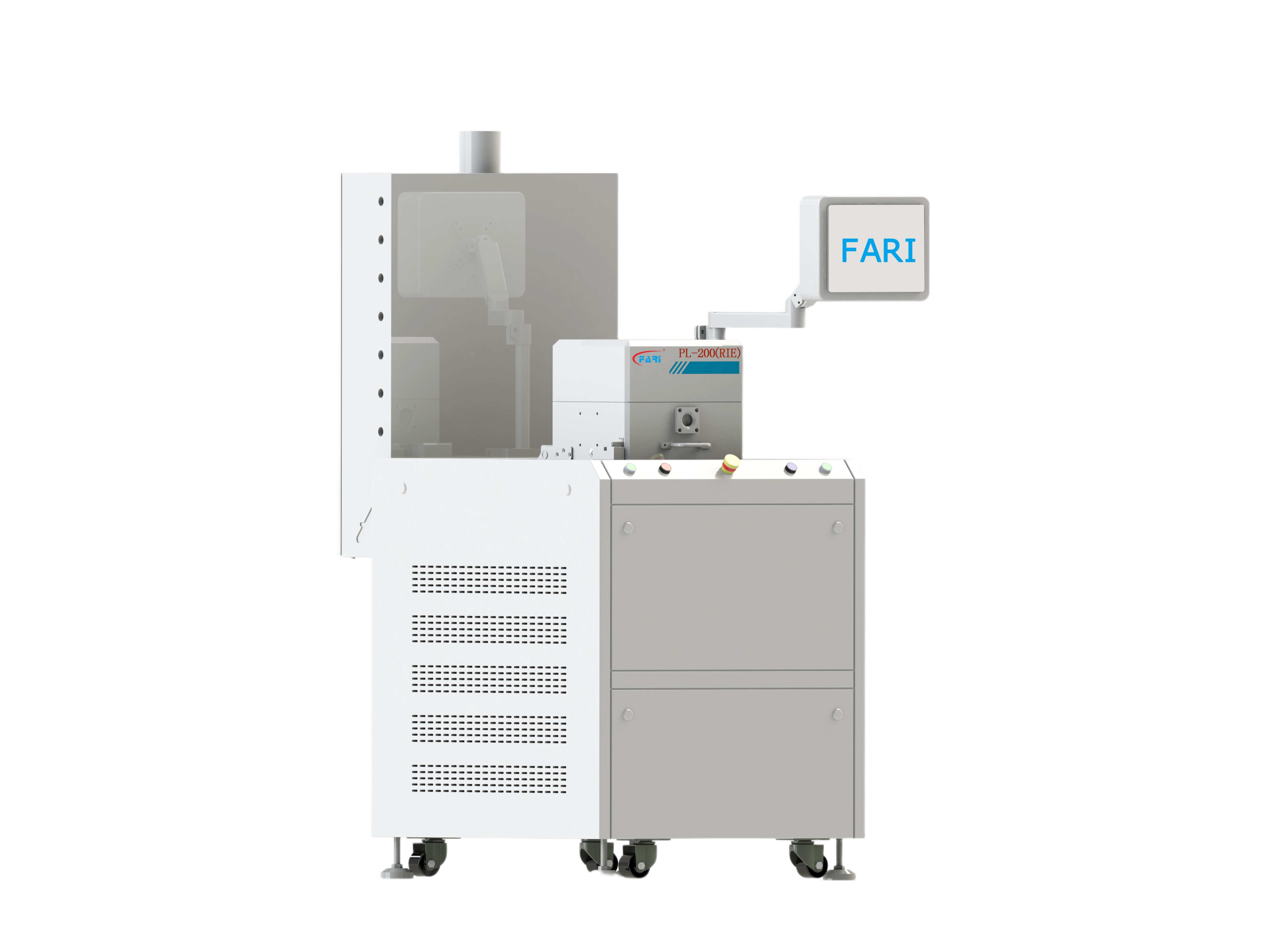
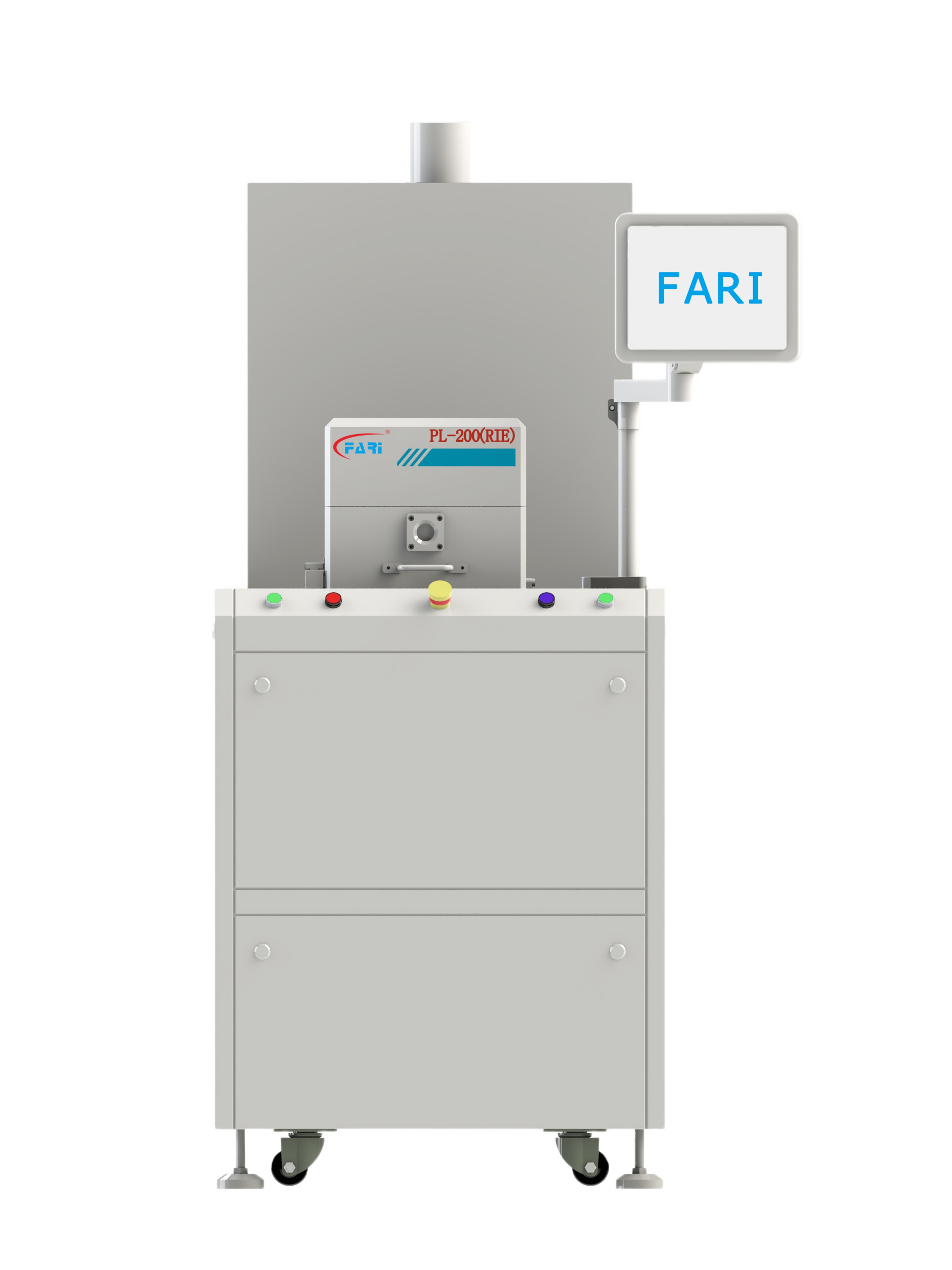
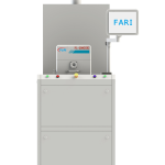
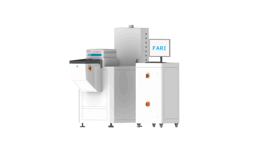
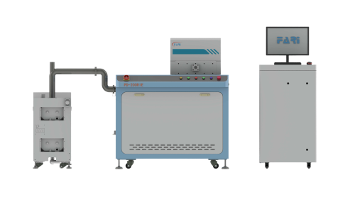
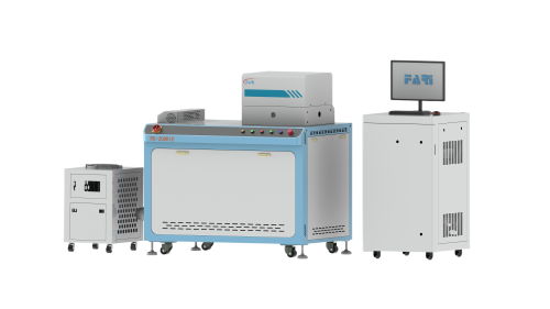
The FR-G200 single-chamber RIE reactive ion etcher delivers precise, anisotropic dry etching for silicon, SiN and SiO2 with high selectivity and repeatability for semiconductor, MEMS and nano-fabrication.
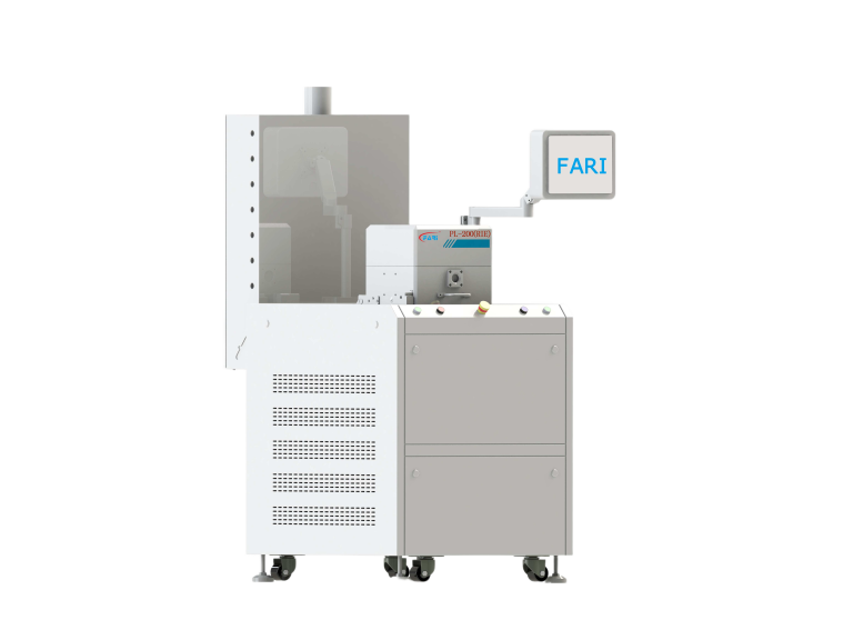
  • Precision anisotropic etching for microfabrication.
  • Single-chamber compact design for lab and pilot use.
  • Broad material compatibility and adaptable chemistries.

Tech Specs

Model FR-G200 (RIE)
Etch Technology Reactive Ion Etching (RIE)
Chamber Type Single-chamber, parallel-plate configuration
Supported Materials Silicon (Si), Silicon Nitride (SiN), Silicon Dioxide (SiO2) and common semiconductor films
Wafer / Substrate Size Up to 200 mm
RF Power Adjustable, 0–600 W
RF Frequency 13.56 MHz
Vacuum Range ≈1x10^-3 to 1x10^-1 Torr (typical process range)
Process Gases CF4, SF6, O2, CHF3, Ar and other specialty chemistries
Etch Mode Anisotropic, ion-assisted chemical etching
Control Interface Digital process controller with recipe storage
Safety & Diagnostics Interlocks, plasma monitoring and fault indicators

Key Features

  • High-Precision Anisotropic Etching

    Provides highly anisotropic reactive ion etching with precise control of ion energy and incidence direction, enabling accurate pattern transfer for submicron features across advanced semiconductor and MEMS processes.

  • Advanced Process Control System

    Integrated RF power delivery and advanced process control enable repeatable recipes, tight endpoint control and stable plasma conditions, ensuring consistent wafer-to-wafer performance for R&D and pilot production.

  • Wide Material Compatibility

    Optimized for silicon, silicon nitride and silicon dioxide, with adaptable gas chemistries and process windows that support etching of a broad range of semiconductor and MEMS materials while preserving selectivity.

  • Compact Single-Chamber Design

    Compact single-chamber configuration minimizes floor space and simplifies maintenance, while maintaining robust vacuum integrity and rapid pump-down times suitable for lab and small-volume manufacturing environments.

  • Excellent Selectivity and Throughput

    Combines high etch rates with excellent selectivity between mask and substrate materials, improving throughput while maintaining tight profile control, sidewall verticality, and low microloading for critical features.

  • Robust Safety and Diagnostics

    Includes safety interlocks, real-time plasma monitoring and diagnostic feedback to facilitate operator safety, rapid fault isolation and predictive maintenance, reducing downtime and protecting substrates.

Plasma Cleaning Process

  • Plasma Generation

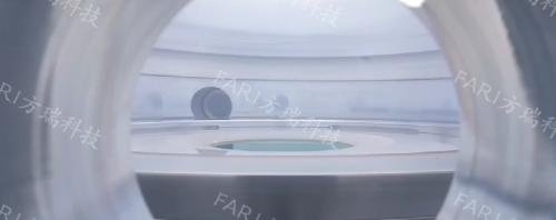
    Process gas is energized and converted into a reactive plasma containing ions, electrons, and radicals.

  • Plasma–Surface Interaction

    High-energy plasma species reach the material surface and interact with contaminants at the molecular level.

  • Chemical Reaction

    Reactive ions and radicals break down organic residues and surface contaminants through controlled chemical reactions.

  • Volatilization

    The reaction products are converted into volatile compounds and enter the gas phase.

  • Removal from Surface

    Gaseous by-products desorb from the surface and are evacuated, leaving a clean, activated material surface.